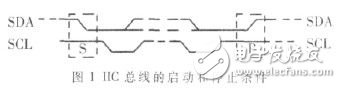
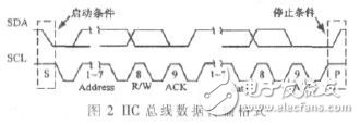
This paper takes the bank's existing queuing system as an example, and proposes the interface design of the MCU queuing system of the IIC bus. Through the simulation test of the system, it not only simplifies the design circuit, reduces the circuit board area, saves the components in the conventional design, and reduces the use. Various costs, as well as system energy consumption, noise cancellation, reliability and other performance are improved. In the MCS-51 series MCU without the IIC bus interface composed of data measurement and control and intelligent instrumentation, the interface device type of the system can be increased through the IIC bus. Reduce system cost and improve application system performance [1-3]. 1 IIC bus The IIC bus (Inter Integrate Circuit Bus) is a bidirectional two-wire bus consisting of a serial clock line (SCL) and a serial data line (SDA). The two wires are connected to different devices with IIC bus. Data transfer between devices, data transfer rate in high-speed mode up to 3.4 Mb / s, not only simplifies the circuit design and improve the efficiency of hardware use, so that the IIC bus is widely used in the serial transmission design of embedded systems, currently mainly used Digital control systems such as central control centers, audio integrated circuits and video. 1.1 IIC bus timing (1) start and stop When the bus is not busy, the clock and data lines remain high. The start condition (S) is when the clock line is at a high level and the data line is at a falling edge. The stop condition (P) is when the clock line is at a high level and the data line is at a rising edge, and the IIC bus starts and stops as shown in FIG. . (2) Data transfer The transmission of one data bit requires one clock pulse, and one flag bit is added after every 1 B. When the flag generated by the transmitter is high level, the master device generates an additional flag bit clock pulse. The information on the data line SDA should be kept stable only when the clock pulse is high, otherwise the data on the data line SDA will become the control signal, as shown in Figure 2. (3) IIC bus protocol Before the IIC bus transmits data, it should indicate the address of the received device. When the IIC bus is started, this address is transmitted together with the 1st transmitted byte. In this system, the PCF8563 chip acts as a slave transmitter or a slave receiver. The SCL signal line is only an input line, and the SDA data line is a two-way signal line. 1.2 Chip PCF8563 Overview PCF8563 is a classic low-power real-time clock/calendar chip [4]. It has IIC bus interface technology. The maximum transfer speed of the bus can reach 400 kb/s. After each write and read data, the internal word address register will be automatically incremented. It has the characteristics of low power consumption and high precision. PCF8563 has timer function, multiple alarm functions, interrupt output function and clock output function, can complete a variety of timing services, can also implement watchdog technology for single-chip system, its internal oscillation circuit, clock circuit, low voltage 1.0 V Detection circuit and IIC two-wire bus communication method, and solve the problem of 2000, not only make the peripheral circuit and its simplicity, but also increase the reliability of the chip, can be widely used in water meters, electricity meters, mobile phones, portable instruments, fax machines , battery power and other product areas. 2 system design 2.1 System Requirements Analysis There are 8 business service windows in the bank service hall. The service window attributes are divided into five types of service business for description, which can carry out personal wealth management business, public business, VIP bank card business, personal deposit and withdrawal savings and collection of mobile phone charges, and hydropower. Mixed services such as fees. Queuing system performance requirements: queues are placed at the entrance of the service hall, so that the depositors can obtain the queue number and print the number in chronological order; the personnel in the service window can realize the call number through the button; after the call, the number is displayed on the screen and the two are continuously through the speaker. Play the number information; the staff can set the relevant (function, mode, menu, etc.) of the queuing system through the background. 2.2 system hardware design The MCU queuing system consists of bank counter operation module, memory module, counter call module, liquid crystal display module and depositor operation module. The system structure is shown in Figure 3. The IIC circuit in the system is used for the interface memory (E2PROM) and real-time precision clock interface [2]. Real-time precision clock uses a lower power CMOS real-time calendar/clock chip, through a divider (for providing source clock to real-time clock RTC), timer, programmable clock output, brownout detector, alarm, and IIC bus Interface to specifically set the precise clock signal necessary for the system. All data and addresses are serially transmitted via the IIC bus interface, and the word address register is automatically incremented each time the data is written and read [5]. The parameter memory (E2PROM) [6] uses a lower power CMOS serial IIC circuit to record information such as counter operations and depositor queues through on-chip memory. Its operational control is fully compliant with the IIC protocol.
Small size Travel Power Strip, easy to carry
with traveling. 1 universal Power Socket, 3 type of Plug EU/AU/US. 4 USB charging ports, 5V 4A output. socket
of grooves on the side, storage power cord, easy to use.You can charge your device more freely on your journey.
Size:145x50x35mm, weight:175g.
PC/ABS flame retardant, phosphor
bronze+pure copper.
Color of socket can be customized.
Travel Power Strip Travel Power Strip, Power Socket, Portable Industrial Socket, Portable Rechargeable Extension Socket ZhongShan JITONGLONG Plastic Hardware Co. Ltd. , https://www.toukoo-electronics.com