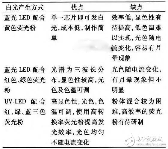
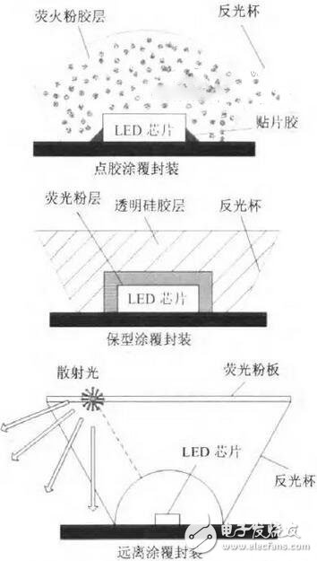
LED (light-emitTIng diode) has become a hot spot for competition in the emerging international strategic industry. In the LED industry chain, the upstream includes substrate materials, epitaxy, chip design and manufacturing, the middle reaches covers packaging technology, equipment and testing technology, and the downstream is LED display, lighting and lighting applications. At present, the blue LED+yellow phosphor process is mainly used to realize the white light high-power LED, that is, a yellow light-emitting YAG (yttrium aluminum garnet) yellow phosphor is emitted by a part of the GaN-based blue LED, and another part of the blue light is emitted through the phosphor. The yellow light emitted by the yellow phosphor is mixed with the transmitted blue light to obtain white light. The blue light emitted by the blue LED chip passes through the yellow phosphor coated around the phosphor, and the phosphor is excited by a part of blue light to emit yellow light, and the blue light spectrum and the yellow light spectrum overlap each other to form white light. As an important part of the industry chain, high-power LED packaging is the core manufacturing technology to promote the practical application of semiconductor lighting and display. Only through the development of low thermal resistance, high luminous efficiency and high reliability LED packaging and manufacturing technology, the LED chip is well mechanical and electrical protection, reducing the impact of mechanical, electrical, thermal, wet and other external factors on the performance of the chip, to ensure LED The stable and reliable work of the chip can provide efficient and continuous high-performance lighting and display effects, realize the unique energy-saving and longevity advantages of LED, and promote the benign development of the entire semiconductor lighting and display industry chain. In view of the consideration of market interests by foreign related companies, the relevant core technologies and equipment are blocked, so the development of independent high-power LED packaging technology, especially white LED packaging equipment, is imminent. This article will briefly introduce the research and application status of high-power LED packaging, analyze and summarize the key technical issues in the process of high-power LED packaging, in order to attract the attention of domestic counterparts, and strive to achieve the autonomy of high-power LED key technologies and equipment. . Packaging process technology plays a crucial role in LED performance. The choice of LED packaging methods, materials, structures, and processes is primarily determined by factors such as chip structure, optoelectronic/mechanical characteristics, specific applications, and cost. With the increase of power, especially the development of solid-state lighting technology, new and higher requirements have been put forward for the optical, thermal, electrical and mechanical structures of LED packages. In order to effectively reduce the thermal resistance of the package and improve the light extraction efficiency, a new technical idea must be adopted for the package design. From the perspective of process compatibility and lowering production costs, the LED package design should be carried out simultaneously with the chip design, that is, the package structure and process should be considered in the chip design. At present, the main development trends of power LED package structure are: miniaturization of size, minimization of device thermal resistance, planar patching, maximum withstand junction temperature, maximizing single-lamp flux; goal is to increase luminous flux, light efficiency, and reduce light. Decay, lose efficiency, improve consistency and reliability. Specifically, the key technologies of high-power LED packaging include: thermal dispersion technology, optical design technology, structural design technology, phosphor coating technology, and eutectic soldering technology. 1, cooling technology The average LED node temperature can't exceed 120 °C. Even the latest devices introduced by LumiLEDs, Nichia, CREE, etc., the maximum node temperature can't exceed 1500 °C. Therefore, the thermal radiation effect of the LED device is basically negligible, and heat conduction and convection are the main ways of heat dissipation of the LED. In the heat dissipation design, heat conduction is first considered because heat is first conducted from the LED package module to the heat sink. Therefore, the bonding material and the substrate are the key links of the LED heat dissipation technology. The bonding materials mainly include three main ways of thermal conductive glue, conductive silver paste and alloy solder. The thermal conductive adhesive is a kind of filler with high thermal conductivity added to the inside of the substrate, such as SiC, A1N, A12O3, SiO2, etc., thereby improving its heat conduction; the conductive silver paste is a composite material formed by adding silver powder into the epoxy resin, and the hardening of the paste is applied. The temperature is generally lower than 200 ° C, which has the advantages of good thermal conductivity and reliable bonding performance, but the absorption of light by the silver paste is relatively large, resulting in a decrease in light efficiency. The substrate mainly includes three main modes of a ceramic substrate, a ceramic substrate and a composite substrate. The ceramic substrate is mainly an LTCC substrate and an AIN substrate. LTCC substrate has many advantages such as easy molding, simple process, low cost and easy to make various shapes. Al and Cu are excellent materials for LED package substrates. Due to the conductivity of metal materials, it is often necessary to pass the surface insulation. Anodizing to form a thin insulating layer on the surface. Metal matrix composites mainly include Cu-based composite materials and Al-based composite materials. Occhionero et al. explored the application of AlSiC on flip-chips, optoelectronic devices, power devices and high-power LED heat-dissipating substrates. The addition of pyrolytic graphite to AlSiC also meets the requirements for higher heat dissipation. There are five main types of composite substrates in the future: monolithic carbonaceous materials, metal matrix composites, polymer matrix composites, carbon composites, and advanced metal alloys. In addition, the package interface has a great influence on the thermal resistance. The key to improving the LED package is to reduce the interface and interface contact thermal resistance and enhance heat dissipation. Therefore, the choice of thermal interface material between the chip and the heat sink substrate is very important. The use of low temperature or eutectic solder, solder paste or conductive paste with nano-particles as the thermal interface material can greatly reduce the interface thermal resistance. 2, optical design technology The optical design of the LED package includes an inner optical design and an outer optical design. The key to internal optical design is the choice and application of potting glue. In the choice of potting glue, it is required to have high light transmittance, high refractive index, good thermal stability, good fluidity and easy spraying. In order to improve the reliability of the LED package, the potting compound is also required to have low hygroscopicity, low stress, temperature and environmental protection. Currently used potting compounds include epoxy resin and silica gel. Among them, silica gel has high light transmittance (high transmittance in the visible range of more than 99%), high refractive index (1.4 to 1.5), good thermal stability (can withstand high temperatures of 200 ° C), and low stress (Young's modulus) Low), low hygroscopicity (less than 0.2%), etc., significantly better than epoxy resin, widely used in high-power LED packaging. However, the performance of silica gel is greatly affected by the ambient temperature, which affects the LED light efficiency and light intensity distribution. Therefore, the preparation process of silica gel needs to be improved. The external optical design refers to the convergence and shaping of the outgoing beam to form a light field with even intensity distribution. It mainly includes reflective concentrator design (primary optics) and shaping lens design (secondary optics). For array modules, it also includes the distribution of chip arrays. Commonly used lenses include convex lenses, concave lenses, spherical mirrors, Fresnel lenses, combined lenses, etc. The assembly method of lenses and high-power LEDs can be airtight and semi-hermetic. In recent years, with the deepening of research, considering the integration requirements after packaging, the lens used for beam shaping uses a microlens array, and the microlens array can play a two-dimensional parallel convergence, shaping, collimation, etc. in the optical path. It has the advantages of high alignment precision, convenient and reliable fabrication, and easy coupling with other planar devices. Research shows that the use of diffractive microlens arrays instead of ordinary lenses or Fresnel microlenses can greatly improve beam quality and increase the intensity of emitted light. LEDs are the most promising new technology for beam shaping. 3, LED package structure LED packaging technology and structure have been in the lead, power package, chip (SMD), chip-on-board (COB) four stages. (1) Lead LED package The LED foot package uses lead frames as pins for various package types. It is the first package structure successfully developed on the market. The variety of products is high, the technology maturity is high, and the structure and reflective layer inside the package are still being improved. Commonly used 3 ~ 5mm package structure, generally used for small current (20 ~ 30mA), low power (less than 0.1W) LED package. It is mainly used for instrument display or indication, and can also be used as a display screen for large-scale integration. The disadvantage is that the package has a large thermal resistance (generally higher than 100K/W) and has a short life. (2) Power LED package The LED chip and package are developed in the direction of high power. Under the high current, the luminous flux is 10-20 times larger than that of the Φ5mm LED. The effective heat dissipation and non-degrading packaging materials must be used to solve the light decay problem. Therefore, the package and the package are also the key. Technology, LED packages that can withstand several W power have emerged. 5W series white, green, blue green, blue power LEDs have been available since the beginning of 2003. The white LED light output reaches 1871m, the light efficiency is 44.31 lm/W green light decay problem, and the LED that can withstand 10W power is developed. Tube; size is 2.5mm X2.5mm, can work at 5A current, light output up to 2001 lm, as a solid illumination source has a lot of room for development. (3) Surface mount (SMD) type (SMD) LED package As early as 2002, surface mount packaged LEDs (SMDLEDs) were gradually accepted by the market, and gained a certain market share. From lead package to SMD, it conformed to the development trend of the whole electronics industry, and many manufacturers introduced such products. SMDLED is currently the highest packaging market share in the LED market. This LED package structure uses an injection molding process to wrap the metal lead frame in PPA plastic and form a reflector cup of a specific shape. The metal lead frame extends from the bottom of the reflector cup to the side of the device. The device pins are formed by flattening outward or inwardly. The improved SMDLED structure is accompanied by white LED lighting technology. In order to increase the power consumption of a single LED device to increase the brightness of the device, engineers began to find ways to reduce the thermal resistance of SMDLED and introduced the concept of heat sink. This improved structure reduces the height of the original SMDLED structure. The metal lead frame is placed directly on the bottom of the LED device. The reflective cup is formed by injecting plastic around the metal frame. The chip is placed on the metal frame. The metal frame is soldered directly through the solder paste. A vertical heat dissipation channel is formed on the circuit board. Due to the development of material technology, SMD packaging technology has overcome the early problems of heat dissipation and service life, and can be used to package high-power white LED chips of 1~3W. (4) COB-LED package The COB package can directly package multiple chips on the metal-based printed circuit board MCPCB, and directly dissipate heat through the substrate, which not only reduces the manufacturing process and cost of the bracket, but also has the advantage of reducing heat dissipation. The PCB can be a low cost FR-4 material (glass fiber reinforced epoxy) or a high thermal conductivity metal based or ceramic based composite (such as an aluminum substrate or a copper coated ceramic substrate). The wire bonding can be performed by thermosonic bonding at high temperatures (gold wire ball bonding) and ultrasonic bonding at normal temperature (aluminum boring tool welding). COB technology is mainly used for LED packaging of high-power multi-chip arrays. Compared with SMD, it not only greatly increases the package power density, but also reduces the package thermal resistance (generally 6-12W/m·K). From the perspective of cost and application, COB will become the mainstream direction of future lighting design. The LED module of the COB package has a plurality of LED chips mounted on the bottom plate. The use of multiple chips not only improves the brightness, but also helps to achieve a reasonable configuration of the LED chips, reducing the amount of input current of a single LED chip to ensure high efficiency. Moreover, the surface light source can greatly expand the heat dissipation area of ​​the package, so that heat can be more easily conducted to the outer casing. The traditional LED luminaire practice is: LED light source discrete device - MCPCB light source module - LED luminaire, mainly based on the practice of not using the applicable core light source components, not only time-consuming, but also costly. In fact, if you take the route of "COB light source module - LED lamp", it can save labor and time, and can save the cost of device packaging. In short, whether it is a single device package or a modular COB package, from low power to high power, the LED package structure is designed around how to reduce the thermal resistance of the device, improve the light output and improve reliability. 4, phosphor coating technology The light conversion structure, that is, the phosphor coating structure, is mainly directed to the LED white light illumination technology, and aims to convert the shorter wavelength light emitted by the LED chip into a longer wavelength light complementary to the complementary color (white color complementary). At present, there are three ways to produce white light by using phosphor: blue LED with yellow phosphor; blue LED with red and green phosphor; UV-LED with red, green and blue phosphors. Among them, commercial white LEDs are mostly single-chip type with blue LED and yellow phosphor. The white light generation method of blue LED with red and green phosphor is only reported in the patents of Osram, Lumileds and other companies, but it has not been commercialized. Products appear, and the way UV-LEDs are combined with three-color phosphors is still under development. The advantages and disadvantages of different phosphors producing white LEDs are shown in the table below. The existing coating methods, as shown in the following figure, each have its advantages and disadvantages. Currently widely used phosphor coating methods are to mix the phosphor with the potting compound and then directly apply it to the chip. Since it is difficult to precisely control the coating thickness and shape of the phosphor, the color of the emitted light is inconsistent, and a blue light or a yellowish light appears. Research by GE's Arik et al. shows that direct phosphor coating on the chip leads to an increase in the temperature of the phosphor, which in turn reduces the quantum efficiency of the phosphor and seriously affects the conversion efficiency of the package. The conformal coating technology based on the spraying process can achieve uniform coating of the phosphor, thereby ensuring uniformity of light color. However, this technique is difficult, and a large part of the blue light emitted by the LED is directly reflected back to the chip by the phosphor layer, thereby being directly absorbed by the chip, which seriously affects the light extraction efficiency. Yamada, Narendran et al. found that the backscattering properties of the phosphors caused 50% to 60% of the forward incident light to be backscattered. In addition, there is a coating method in which the phosphor layer is away from the LED chip (for example, the phosphor layer is located on the reflector or astigmatism cup outside the LED chip), and the amount of light absorbed by the phosphor layer reflected back to the chip can be greatly reduced. , thereby improving the light extraction efficiency. In addition, since the phosphor layer is not in direct contact with the chip, the heat generated by the chip is not transferred to the phosphor layer, thereby prolonging the life of the phosphor layer. A study by Schubert et al. at Leinster Institute of Technology found that using a far away phosphor coating process can reduce the probability that light that is dissipated backwards is absorbed by the chip, and can increase the luminous efficiency of the LED by 7% to 16%. Wang Gang and others from Sun Yat-sen University also conducted related research. The results show that the use of far-off phosphor coating can reduce the phosphor coating temperature by about 16.8 ° C, which significantly improves the conversion efficiency of the phosphor. However, there is a disadvantage in that it is far from the coating method, because the cost of using the phosphor powder is relatively large, and the manufacturing and installation process of the phosphor plate is relatively complicated, and it is currently not widely available and industrially applied. In addition, on the basis of studying the optimization of phosphor coating, You et al. proposed to use a multi-layer phosphor structure to separate the red phosphor layer from the yellow phosphor layer, and the yellow phosphor on the red phosphor. The experimental results show Such a phosphor coating structure can reduce the mutual absorption between the phosphor coatings, and the lumen efficiency of the packaged product can be improved by 18%. 5, eutectic welding technology Eutectic soldering technology is one of the most critical core technologies in high-power LED flip chip packaging. The advantages of eutectic soldering technology in the LED packaging process, the core heat dissipation problem and the solid crystal problem, are and will become the mainstream direction of LED packaging development in the future. The eutectic alloy has a lower melting point than the pure component, and the melting process is simple; the eutectic alloy has better fluidity than the pure metal, and prevents dendrite formation which hinders liquid flow during solidification, thereby improving casting properties; eutectic alloy It also has a constant temperature transition characteristic (no solidification temperature range), which can reduce casting defects such as segregation and shrinkage; the toughness of the eutectic alloy after curing is close to the toughness of the metal, and it is not suitable for fracture; The microstructure, especially the regular arrangement of layered or rod-like eutectic structures, can be an in-situ composite of superior performance. Because of the many advantages of eutectic, LED packages fabricated using eutectic processes have the advantage of reducing impedance and improving heat transfer efficiency. Multifunction Steam Rice Cooker,Kitchen Rice Cooker,Kitchen Rice Cooker,Automatic Rice Cooker JOYOUNG COMPANY LIMITED , https://www.globaljoyoung.com