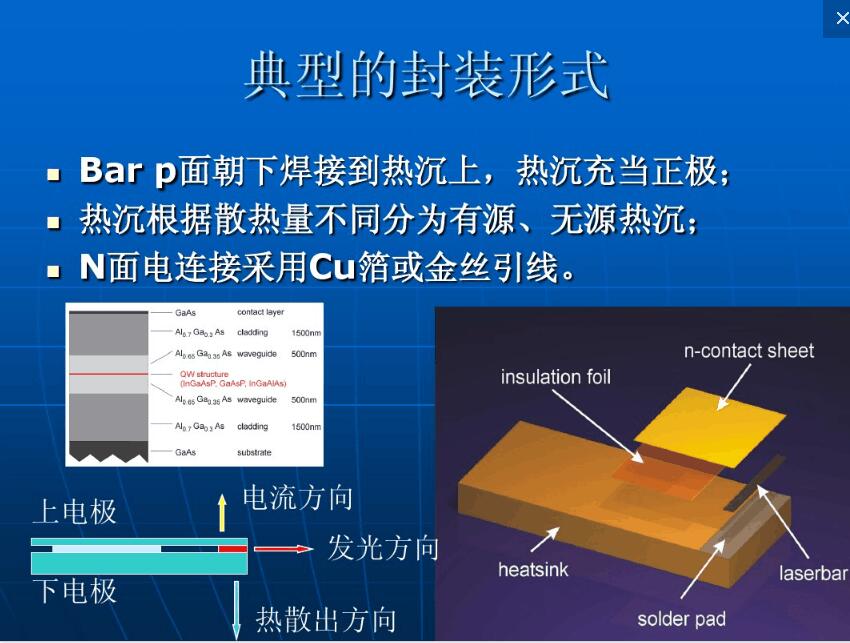
Semiconductor lasers are lasers that use semiconductor materials as working substances. Due to differences in material structure, the specific processes for generating lasers of different types are special. Commonly used working substances are gallium arsenide (GaAs), cadmium sulfide (CdS), indium phosphide (InP), and zinc sulfide (ZnS). The excitation methods are three forms: electric injection, electron beam excitation and optical pumping. Semiconductor laser devices can be classified into homojunction, single heterojunction, and double heterojunction. Homogeneous junction lasers and single heterojunction lasers are mostly pulsed devices at room temperature, while double heterojunction lasers can operate continuously at room temperature. Semiconductor lasers rely on injected carriers. There are three basic conditions for emitting lasers: (1) To generate a sufficient population inversion distribution, that is, the number of high-energy particles is sufficiently larger than the number of particles in the low-energy state; (2) There is a suitable resonant cavity that can play a role in feedback, so that the excited radiation photons proliferate, thereby generating laser oscillation; (3) To meet certain threshold conditions, so that the photon gain is equal to or greater than the loss of photons. The working principle of the semiconductor laser is an excitation method. The semiconductor material (that is, using electrons) is used to illuminate between the energy bands, and the cleavage plane of the semiconductor crystal is used to form two parallel mirror surfaces as mirrors to form a resonant cavity to oscillate and feedback the light. The radiation that produces the light is amplified and the laser is output. Advantages of semiconductor lasers: small size, light weight, reliable operation, low power consumption, high efficiency, etc. In general, the wavelength of the light emitted by the semiconductor laser varies from 0.2 to 0.3 nm/° C., and the spectral width increases, which affects the color vividness. In addition, when the forward current flows through the pn junction, the heat generation loss causes the junction region to generate a temperature rise. At room temperature, for every 1 °C increase in temperature, the luminous intensity of the semiconductor laser is reduced by about 1%, and the package is cooled. Color purity and luminescence intensity are very important. In the past, the method of reducing the driving current was used to reduce the junction temperature. The driving current of most semiconductor lasers was limited to about 20 mA. However, the light output of semiconductor lasers increases with the increase of current. Many power semiconductor lasers can drive currents up to 70mA, 100mA or even 1A. It is necessary to improve the package structure, the new semiconductor laser package design concept and low thermal resistance package structure. And technology to improve thermal properties. For example, a large-area chip flip-chip structure is used, and a silver paste with good thermal conductivity is used to increase the surface area of ​​the metal support, and the silicon carrier of the solder bump is directly mounted on the heat sink. In addition, in the application design, the thermal design and thermal conductivity of the PCB circuit board are also very important. After entering the 21st century, the efficiency, high brightness and full colorization of semiconductor lasers are constantly developing and innovating. The red and orange semiconductor lasers have achieved 100Im/W, and the green semiconductor lasers have 501m/W. The luminous flux of single semiconductor lasers. It also reaches tens of Im. Semiconductor laser chips and packages no longer follow the traditional design concept and manufacturing mode of Gong. In terms of increasing the light output of the chip, research and development is not limited to changing the amount of impurities in the material, lattice defects and dislocations to improve internal efficiency, and at the same time, how Improve the internal structure of the die and package, enhance the probability of photon emission inside the semiconductor laser, improve the light efficiency, solve the heat dissipation, take light and heat sink optimization design, improve the optical performance, accelerate the surface mount SMD process is also developed by the industry Mainstream direction. 1. The VCSEL chip is attached to the surface of the gold-plated heat sink, and the positive and negative electrodes of the chip are taken out by the process of gold wire bonding, and then the chip is turned over and fixed by 90°; 2, using the working principle of the refrigerator, so that the working temperature of the laser chip is always maintained in the range of 24 ° C ± 1 ° C; 3. Use a thermistor with a negative temperature coefficient to monitor the working current of the refrigerator at all times; 4. Directly coupled to the chip with a metallized fiber; 5. Fixing the optical fiber by laser welding process; 6. The coupling device is first subjected to high-temperature storage for 8 hours, and then subjected to high-temperature cycle for 24 hours to ensure the release of laser welding stress; 7. Seal the device with a parallel sealer. The invention has the following advantages: the chip has high luminous efficiency, high fiber output power, high straight-through rate, good stability and long service life. Semiconductor lasers are early-stage and fast-developing lasers. Due to their wide wavelength range, they are simple to manufacture, low in cost, easy to mass-produce, and because of their small size, light weight and long life, the variety is developing rapidly. It has a wide range of more than 300 kinds. The most important application field of semiconductor lasers is Gb LAN, and 850nm wavelength semiconductor lasers are suitable for 1Gh/. LAN, 1300nm -1550nm wavelength semiconductor laser is suitable for 1OGb LAN system. The application range of semiconductor lasers covers the entire field of optoelectronics and has become the core technology of today's optoelectronics science. Semiconductor lasers have been widely used in laser ranging, laser radar, laser communication, laser analog weapons, laser warning, laser guidance tracking, ignition detonation, automatic control, and detection instruments, forming a broad market. In 1978, semiconductor lasers began to be used in fiber-optic communication systems. Semiconductor lasers can be used as light sources and indicators for fiber-optic communications and as optical subsystems through large-scale integrated circuit planar processes. Due to the ultra-small, high-efficiency and high-speed operation of semiconductor lasers, the development of such devices has been closely integrated with optical communication technology since the beginning, in optical communication, optical conversion, optical interconnection, parallel optical wave systems, Optical information processing and optical storage, optical disasters of optical computer peripherals, etc. have important applications. The advent of semiconductor lasers has greatly promoted the development of information optoelectronic technology. Today, it is the most important and most important source of laser fiber communication in the field of optical communication. Semiconductor lasers, coupled with low-loss optical fibers, have had a major impact on fiber-optic communications and have accelerated its development. Therefore, it can be said that without the emergence of semiconductor lasers, there is no current optical communication. GaAs/GaAlA. Double heterojunction lasers are important sources of optical fiber communication and atmospheric communication. Today, distributed optical semiconductor transmission systems (DFB-LD) are used for long-haul, large-capacity optical information transmission systems. Semiconductor lasers are also widely used in optical disc technology, which is a comprehensive technology integrating computing technology, laser technology and digital communication technology. It is a high-density, fast, efficient, and low-cost means of information storage. It requires a beam generated by a semiconductor laser to write and read information.
Asic Miner Bitmain:Asic Miner Bitmain Ka3 166Th Kda Mining Machine
Bitmain is the world's leading digital currency mining machine manufacturer. Its brand ANTMINER has maintained a long-term technological and market dominance in the industry, with customers covering more than 100 countries and regions. The company has subsidiaries in China, the United States, Singapore, Malaysia, Kazakhstan and other places.
Bitmain has a unique computing power efficiency ratio technology to provide the global blockchain network with outstanding computing power infrastructure and solutions. Since its establishment in 2013, ANTMINER BTC mining machine single computing power has increased by three orders of magnitude, while computing power efficiency ratio has decreased by two orders of magnitude. Bitmain's vision is to make the digital world a better place for mankind.
Asic Miner Bitmain,Ka3 166Th Kda,Kda Miner Antminer Ka3,Asic Miner Ka3,ka3 miner Shenzhen YLHM Technology Co., Ltd. , https://www.sggminer.com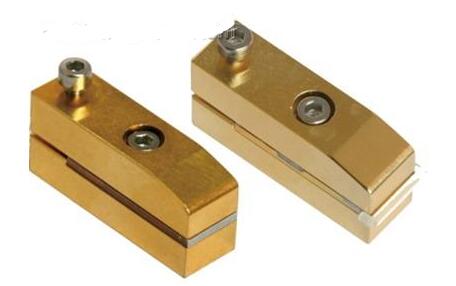
Semiconductor laser concept