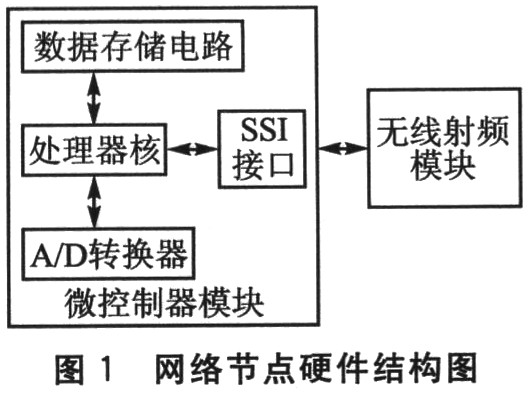
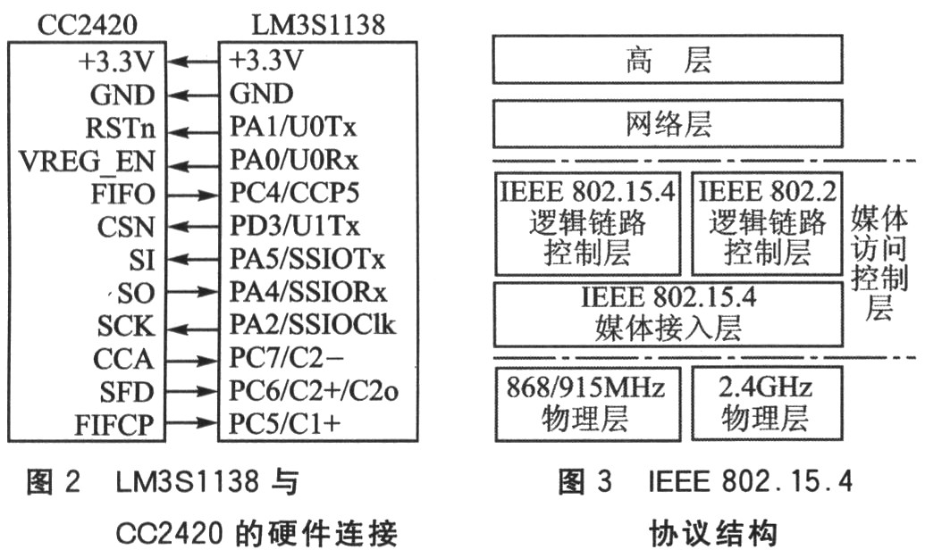
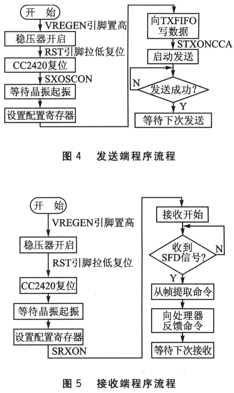
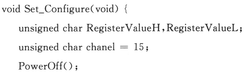
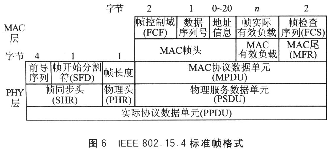
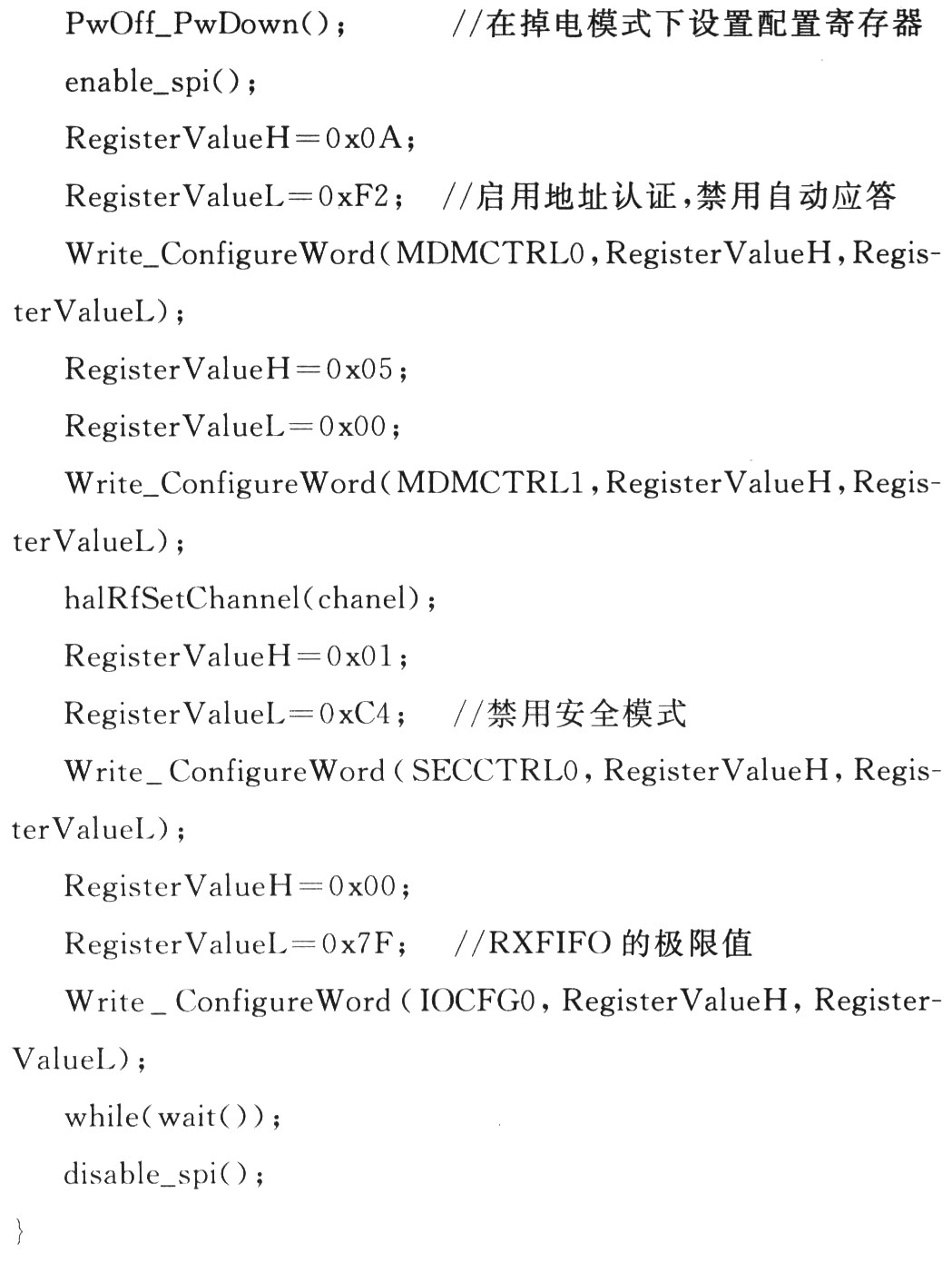
LM3S1138 and CC2420 wireless sensor network communication introduction Wireless sensor network (Wireless Sensor Network, WSN) is a comprehensive intelligent information system that integrates information collection, information transmission, and information processing. It consists of a large number of inexpensive micro sensor nodes deployed in the monitoring area. It is a multi-hop self-organizing network formed by wireless communication. It has the characteristics of low power consumption, low cost, distribution, self-organization, rapid deployment, and strong resistance to destruction. The wireless sensor network can monitor the system in real time and feed back information in time to achieve complex target detection and tracking in a specified range, and has a broad application space. This article introduces the method of using LM3S1138 microcontroller and CC2420 wireless radio frequency chip to construct a wireless sensor network node, and explains how to achieve point-to-point communication transmission. 1 Hardware node design 1.1 Network node design A wireless sensor network consists of multiple network nodes in the network. With a modular design method, the hardware of the node consists of a microcontroller module and a radio frequency module. Among them, the microcontroller module includes processor core, data storage circuit and A / D converter, etc., and other sensor modules can be connected according to different needs. The network node hardware structure is shown in Figure 1. 1.2 LM3S1138 microcontroller The microcontroller uses LM3S1138 from Luminary. It uses a Cortex-M3 processor core with 32-bit RISC structure, with 64 KB single-cycle Flash, 16 KB single-cycle access SRAM, 4 general-purpose timer modules (GPTM) (each provides 2 16-bit timers), 16-bit ADC event trigger, ARM FiRM compatible watchdog timer, 2 synchronous serial interfaces (SSI), 3 fully programmable 16C550 UARTs (support IrDA), 3 independent integrated analog comparators, 2 I2C modules, 9 to 46 GPIOs (the specific number depends on the configuration), on-chip low dropout (LDO) voltage regulator (with programmable output voltage, user adjustable range is 2.25 to 2.75 V ), A test access port (TAP) controller that complies with the IEEE 1149.1-1990 standard (debug access via JTAG and serial interface, complete JTAG boundary scan), 6 reset sources, and programmable clock source control ( The clock of a single peripheral can be gated to reduce power consumption). Cortex-M3 is a low-power embedded processor designed by ARM for deeply embedded applications that require fast interrupt response capabilities. It has the characteristics of few gates, short interrupt delay and low debugging cost. It adopts ARMv7-M architecture and is a synthesizable and highly configurable processor. Cortex-M3 contains an efficient Harvard structure three-stage pipeline, can provide 1.25 DMIPS / MHz, operating frequency is 50 MHz, using Thumb-2 instruction set compatible with Thumb instructions to obtain higher code density. It uses hardware division and single-cycle multiplication; integrated nested vector interrupt controller (NVIC), 34 interrupts have 8 priority levels; with optional memory protection unit (MPU), provides a privileged mode to protect the function of the operating system; Unaligned data access allows data to be placed in memory more efficiently; precise bit-banding not only maximizes memory space, but also improves peripheral control. The hardware platform of this article selects the EasyARM1138 development board with LM3S1138 as the main control chip. 1. 3 CC2420 wireless radio frequency chip The CC2420 wireless radio frequency chip is a 2.4 GHz radio frequency chip developed by Chipcon that conforms to the ZigBee standard. The chip is a product compatible with the ZigBee protocol / IEEE 802.15.4 standard designed for low power consumption. It provides extended hardware to implement information processing, data cache, burst transmission, data encryption and decryption, data identification, and channel idle confirmation. , Connection quality assessment and packet time information. These features reduce the burden on the host, making CC2420 can be connected with a low-speed low-cost microcontroller, and through the SPI interface can easily control and data access to CC2420. 1.4 Hardware connection between LM3S1138 and CC2420 According to Zhou Ligong's EasyARM1138 development board using the SSI port to simulate the characteristics of SPI and the working principle of CC2420, the hardware connection between LM3S1138 and CC2420 is shown in Figure 2. Because the CC2420 module uses the SPI interface to communicate with the host, and the EasyARM1138 uses the SSI interface to simulate the SPI transmission, in the frame format provided by the SSI port on the development board, the frame format of Freescale SPI when SPO = 0 and SPH = 0 is selected. But in this frame format, the chip select signal SSIFss does not comply with the SPI communication rules of the CC2420 module, so another pin is selected to simulate the SPI chip select signal, namely the PD3 / U1Tx pin. 2 IEEE 802.15.4 Standard The IEEE Standards Committee formally approved and established the 804.15.4 working group in December 2000. Its task is to develop a low data rate WPAN standard in order to meet the requirements of low-power and low-cost wireless networks. IEEE802. 15.4 is a standard-based protocol that provides the required network infrastructure for wireless sensor network applications; it has the characteristics of low complexity, low cost, and low power consumption, and can perform low data rates between low-cost devices Transmission. The standard meets the International Standards Organization (ISO) Open System Interconnection (OSI) reference model, including the physical layer, media access control layer, network layer, and high-level. IEEE802. 15.4 defines the physical layer (PHY) and the media access control layer (MAC). The protocol structure is shown in Figure 3. 3 Communication software design 3.1 Overall design The CC2420 module uses the SPI interface to communicate with the host, so in this design, the EasyARM1138 development board is used as the host, and the CC2420 module is used as the slave, respectively as the sender and receiver. First initialize the CC2420 through the SPI pin on the development board; then configure the corresponding registers in the CC2420 chip and define the data format used in the communication; finally set the channel and start sending. 3. 2 software design of sending end and receiving end To achieve point-to-point communication is to realize the functions of the sending end and the receiving end, so that the two nodes can freely exchange information. The following mainly introduces the method of its realization. 3.2.1 Program flow of the sender and receiver The program flow of the sender and receiver is shown in Figure 4 and Figure 5, respectively. 3.2.2 Chip initial configuration Before using CC2420 for wireless data transmission, some configuration must be made as needed. After SPI is enabled, the microcontroller sends commands to the CC2420, and these commands are transmitted to the CC2420 through the simulated SPI interface. In this way, users can configure the value of the register according to their needs, choose whether to use address authentication, security authentication and other functions, and also need to set up the sending and receiving channels. There are 16 selectable channels provided under 2.4 GHz, the initialization procedure is as follows: 3.2.3 Realization of the program at the sending end and the receiving end It can be seen from the program flow that both the sending end and the receiving end need to initialize the pins and chips first, and wait for the CC2420 crystal oscillator to start, and then configure the registers according to the needs of the program. At the sending end, you need to send the data to be transmitted to the TXFIFO of the CC2420 through the SPI interface of the microcontroller to buffer it. This needs to be sent according to the custom or IEEE 804.15.4 defined frame format. After the data is cached You can start sending. This design uses the IEEE standard frame format, in the frame structure Preamble Se-quence, SFD and FCS are automatically generated by the hardware when sending. The frame format is shown in Figure 6. Charger,usb-c charger,type c charger,USB Charger,phone charger Dongguan Aiqun Industrial Co.,Ltd , https://www.gdoikwan.com