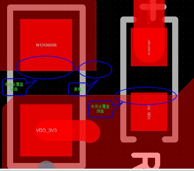
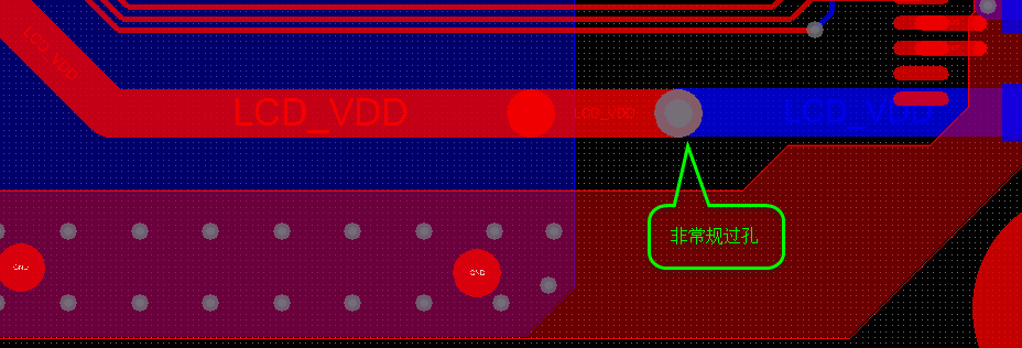
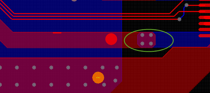
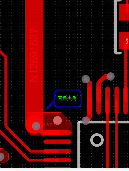
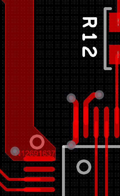
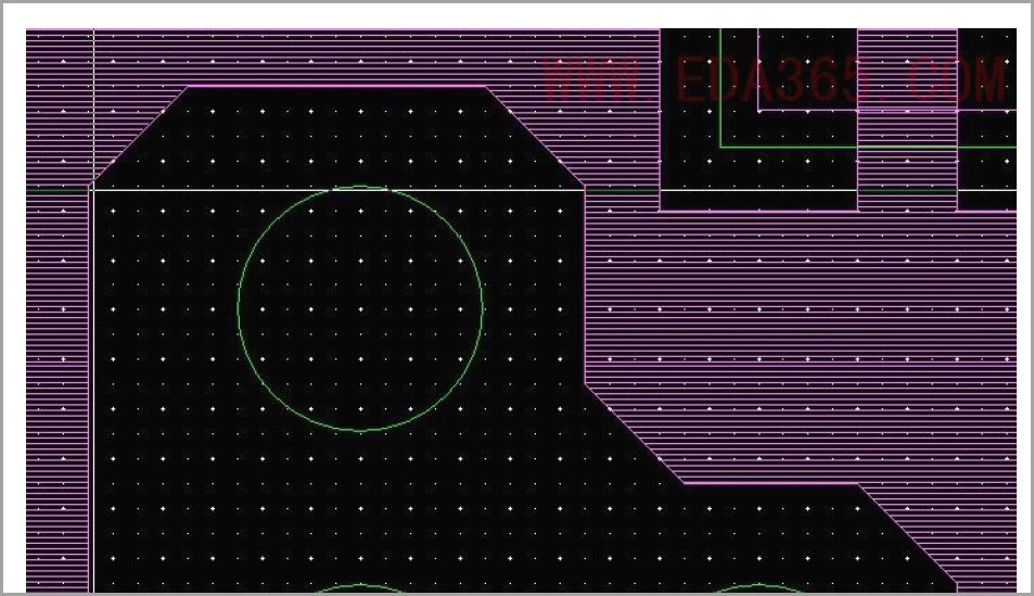
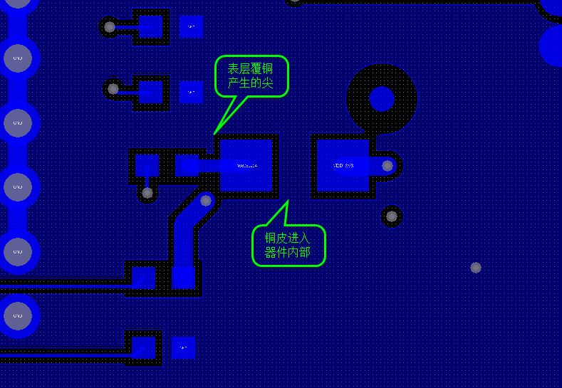
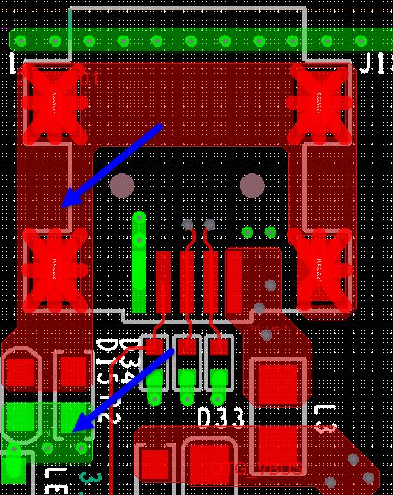
1. When the copper cover covers the pad, it must be completely covered. The shape and pad cannot form an acute angle. 2. Try to use copper instead of thick wire. When using thick lines, the vias are usually best not to trace through vias, increasing the via hole and pad. After modification: 3. Try to replace the pattern of copper and copper traces with copper. The latter often produces some small sharp corners and right angles. Replace copper traces with copper: After modification The boundary of 4.shape must be on the grid point, grid-off is not allowed. (sony specification) 5. Shape corners must be of the same size. As shown in the figure below, both corners of the corner are 4 grid points, so all the small corners must do this. (sony specification) The shape cannot cross the pad and enter the interior of the device. In particular, the surface layer is covered with copper. (sony specification) 8. Strictly speaking, shape & shape, shape & line must be equally spaced. If you set the shape and line 0.3mm, spacing, then all shape spacing should be so, there can be no case such as 0.4mm or 0.25mm, but Keeping the grid copper is the spacing of grids on the premise of meeting the 0.3mm spacing. (sony specification) 9. The ground of the plug, and the inductance and resistance connected to the housing ground, the GND on the other side of the resistance, preferably copper 10. It is better to use an 8-corner method instead of the Full Connect method 11. The GND terminal of the capacitor is best to enter the inner ground directly through the via hole. Do not connect through the copper skin. The latter is not conducive to welding, and the copper skin in the small area is meaningless. 12. The connection of the power supply, especially the power pin output from the power chip is preferably connected by copper 13.PCB, even if there are a large number of blank areas, if the spacing of the signal lines is large enough, no surface copper clad ground is needed. The partial copper coating on the surface will cause uneven balance of the copper foil on the circuit board. And if copper is too close to the trace, the impedance of the trace will be affected by the copper. 14. Due to space constraints, GND cannot be approached through the via to the inner ground. This can be done through partial copper and then through the via and the inner ground. Acetate Glasses,Acetate Sunglasses,Acetate Eyeglasses,Acetate Round Sunglasses Danyang Hengshi Optical Glasses Co., Ltd. , https://www.hengshi-optical.com