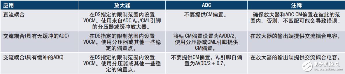
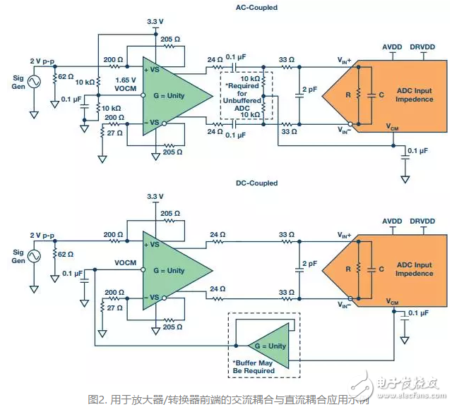
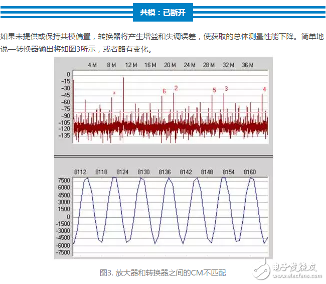
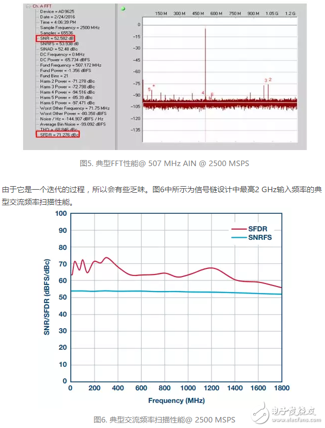
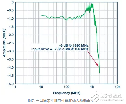
In the field of converters, it is impossible to mention the GSPS ADC - also known as RF ADC. There has been a lot of discussion about the advantages of using RF ADCs and how to design them and capture data at high rates. However, people seem to have forgotten one thing, low DC signal. The input configuration or front-end design prior to a high-performance ADC is critical to achieving the desired system performance. The usual focus is on capturing broadband frequencies, such as broadband frequencies greater than 1 GHz. However, in some applications, DC or near DC signals are also required and are popular with end users as they can also transmit important information. Therefore, capturing DC and wideband signals by optimizing the overall front-end design requires a DC-coupled front end that is always connected to the high-speed converter. Given the nature of the application, an active front-end design will need to be developed because the passive front end used to couple the signal to the converter and the balun itself are ac-coupled. Next, we take the actual system solution as an example to outline the importance of the common mode signal and how to properly level shift the front end of the amplifier. You can also think of it as a new midpoint or zero code—amplifier, usually with a VOCM pin or similar device that builds the CM at the output. Be careful, however, that these pins also have certain current and voltage range requirements. It is best to consult the amplifier data sheet and/or use a stable bias point that will not overload any adjacent circuitry or reference point inside the circuit. Do not just tap the voltage reference pin (VREF) of a converter, which is usually half the full scale of the converter. A full high precision offset may not be available. For your discretion, you should also consult the pin specifications on the converter data sheet. In general, a simple voltage divider and/or buffer driver with a 1% resistor tolerance can correctly set the CM bias of the amplifier. A brief description of how to connect the amplifiers and converters for each application is given in Table 1 below. Figure 2 shows some examples of the correct circuit. The shape of the output spectrum will be similar to the overload full-scale input. This means that the zero point of the converter is off center and not optimal. You may find that the converter will clip earlier or not reach the full scale of the converter. However, this problem has become more serious as the converter begins to use a 1.8 V supply and a lower power supply. This means that the CM bias of the analog input is 0.9 V or AVDD/2. Not all single-supply amplifiers support such low common-mode voltages while still maintaining relatively good performance. However, not any older amplifier can be used because the margin can be very limited and the internal transistors may begin to collapse. If dual power supplies are used with the amplifier, in most cases there should be sufficient headroom to achieve the proper CM bias. The downside is the addition of an extra power supply - possibly a standard negative supply, which means more devices and higher costs. A simple inverter circuit helps solve this problem. In this configuration shown, the front-end interface is optimized for wideband sampling while preserving the DC component of the signal. Since the device is +5.5 V withstand voltage. This design uses +3.3 V and −2 V AVDD to separate the power supplies. This allows a simple alignment of the common mode between the output of the amplifier and the input of the ADC, both of which must be +0.525 V at AIN+ and AIN−. Also, note the several ground-enabled amplifier pin functions (VSS), which are now forced to be set to −2 V supply (new VSS). The CM voltage output is simple, but figuring out the common mode requirements of the amplifier inputs can be a bit of a hassle. Need to do two things for the interface: 1. The input CM voltage needs to be configured to 0 V. Otherwise, the driver amplifier offset will bias the output rail to one side. This will result in a performance problem as described in Figure 3 or more severely - there will be poor AC performance in the amplifier and converter signal chains. To this end, each side of the amplifier input needs to allow current to flow to the ground, or 2 V in this DC coupling case. Therefore, a 2.2 kΩ resistor is added to each amplifier input to suppress the offset current. How it works: The amplifier output is approximately 0.525 V and the amplifier input CM voltage is 0 V. With an internal feedback resistance of 500 Ω and an input resistance of approximately 50 Ω, it appears to have 550 Ω; or in this example, we assume a 50 Ω source resistance in parallel with a 100 Ω resistor, resulting in 33 Ω. Then add 20 in series to increase to 53 ?. This is a series of 500? internal feedback resistors or a total of 553?. That is, a 0.525 V resistor divider of 500 ? and 53 ? is formed. In turn, a current of 900 μA (or 0.525/553) is produced. To shunt this to ground or to a new VSS or −2 V, add a 2.2 kΩ resistor or −2 V/2.2 kΩ = 900 μA. 2. The input is a single-ended input and needs to be properly configured to maintain optimum performance while maintaining low even-order distortion. Similarly, the 100? and 50? source resistances are effectively paralleled to obtain 33.33? Thevenin equivalent resistance, as previously described. This is usually reflected in the VIN node to balance the input to the device because it is single-ended. However, to improve even-order distortion, 20 Ω on the VIN+ node is used to maintain low distortion for all wideband frequencies. This is done by using a specific intermediate frequency of approximately 500 MHz—or see the test example in Figure 5. It is worth noting that a 5.1 nH inductor is added in series with the positive rail input of the power supply. This helps to improve even-order linearity performance and frequency again by capturing and recycling these unbalanced currents inside the amplifier. Finally, the interface needs to be optimized for the front-end BW between the amplifier and the ADC. This is usually done in an iterative manner as well. However, there are a few points to note about the setting of certain values ​​between two ICs. In order to get the best BW in the interface, please follow the rules below - Select a kickback resistor (RKB), (in this case, ?), based on experience and / or ADC data sheet recommendations, usually between 5 ? and 36 ?. Select the external series resistance (RA) of the amplifier. If the amplifier's differential output impedance is in the range of 100 Ω to 200 Ω, RA should be less than 10 Ω. If the amplifier output impedance is 12 ? or lower, RA should be between 5 ? and 36 ?. At this point, select a 10? series resistor and a differential output with an impedance of 10 Ω for the ADL5567. The series and shunt total resistance of the amplifier output should be close to the amplifier's characterized load (RL). Here, the circuit in Figure 4 is 160 ?, or 2 RA + 2 RKB + RADC = 20 +40 + 100. The ADL5567 has a 200 Ω RL, so if the design value deviates too much from the amplifier's RL characteristic value, the linearity performance may deviate. Add the internal ADC capacitor CADC to the shunt capacitor after the 10? series resistor to help complete the internal ADC sampling network kickback. This also provides soft low pass filtering to reduce the wideband harmonics in any foldback band. A 2 GHz passband flatness response product was developed using the above criteria to capture frequencies in the 1st and 2nd Nyquist zones, assuming a sampling rate of 2.5 GSPS. The input drive specification for this design will be −8 dBm or 252 mV pp, assuming 50 μΩ input impedance at 100 MHz reference frequency. This is the input full-scale level at which the amplifier input requires the converter to reach full scale. In any DC-coupled design, ignoring the converter's common-mode input voltage specifications can cause serious problems. If multiple levels are used, the common mode levels in the signal chain must be consistent to prevent the two components from colliding with each other. If not properly coupled, one of them will often win between levels, producing false measurements. For AC-coupled applications, a coupling capacitor is used between the two stages to break this common-mode mismatch. This design optimizes the bias of the amplifier output and the ADC input. Otherwise, dual power or level shifting circuits should be considered in the system design, as described in the DC coupling design above.
Vibration Motor is in the original basis to add a vibrating head, made into a Dc Motor drive with a vibration motor. To produce the shaking force.
6V Dc Vibration Motor is introduced:
6V Dc Vibration Motor volume is generally greater than 15 mm, mainly used in massage chair, massage waist, handheld massager, etc.
Characteristics: small volume, strong vibration;
Operating temperature range:
6V Dc Vibration Motor should be used at a temperature of -10~60℃.
The figures stated in the catalog specifications are based on use at ordinary room temperature catalog specifications re based on use at ordinary room temperature (approximately20~25℃.
If a vibration motor is used outside the prescribed temperature range,the grease on the gearhead area will become unable to function normally and the motor will become unable to start.Depending on the temperature conditions ,it may be possible to deal with them by changing the grease of the motor's parts.Please feel free to consult with us about this.
Storage temperature range:
Dc Vibration Motor should be stored ta a temperature of -15~65℃.
In case of storage outside this range,the grease on the gearhead area will become unable to function normally and the motor will become unable to start.
Service life:
â—Use with a load that exceeds the rated torque
â—Frequent starting
â—Momentary reversals of turning direction
â—Impact loads
â—Long-term continuous operation
â—Forced turning using the output shaft
â—Use in which the permitted overhang load or the permitted thrust load is exceeded
â—A pulse drive ,e.g.,a short break,counter electromotive force,PWM control
â—Use of a voltage that is nonstandard as regards the rated voltage
â—Use outside the prescribed temperature or relative-humidity range,or in a special environment.
â—Please consult with us about these or any other conditions of use that may apply,so that we can be sure that you select the most appropriate model.
when it come to volume production,we're a major player as well .each month,we rurn out 600000 units,all of which are compliant with the rohs directive.Have any questions or special needed, please contact us, we have the engineer group and best sales department to service to you Looking forward to your inquiry. Welcome to our factory.
6V Dc Vibration Motor,Dc Vibration Motor,6V Dc Micro Vibration Motor,Small Size 6V Dc Vibration Motor Shenzhen Shunchang Motor Co., LTD. , https://www.scgearmotor.com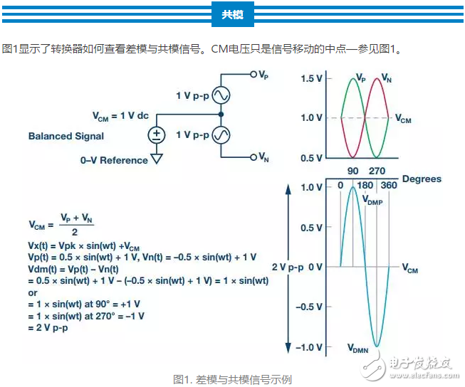
Features: small size, fast speed, stable performance, low price, can use battery drive,Can change the different materials of the pendulum head


Method of use: the best stable in horizontal plane, installed on the dc 6V Dc Vibration Motor output shaft parts, cannot use a hammer to knock, knock prone to press into the dc 6V Dc Vibration Motor drive, may cause damage to internal components, and cannot be used in the case of blocked.

