Doping trivalent elements such as boron into pure silicon crystals to replace silicon atoms in the crystal lattice to form a P-type semiconductor. In P-type semiconductors, holes are multi-character, and free electrons are minority carriers, and holes are mainly used for conduction. The more impurities doped, the greater the concentration of holes and the stronger the conductivity. The pure silicon crystal is doped with a 5-valent element such as phosphorus to replace the position of the silicon atom in the crystal lattice to form an N-type semiconductor. In N-type semiconductors, the concentration of free electrons is greater than the concentration of holes, so free electrons are multiple sons, and holes are minority sons. As shown below: When the P-type semiconductor and the N-type semiconductor are joined together, since the hole concentration in the P-type semiconductor is high, and the electron concentration in the N-type semiconductor is high, a diffusion movement will be formed, and the holes in the P-type semiconductor will move to its low concentration. The electrons of the N-type semiconductor will also diffuse to the place where its concentration is low, and thus diffuse to the P-type region. In this way, the negative ions that cannot move freely remain in the P-type region, and the positive ions that cannot move freely remain in the N-type region. One positive and one negative form an internal electric field from left to right inside the PN junction. This internal electric field reflects the working characteristics of the PN junction. Another point to note is that the PN junction is only partially charged, that is, the P-type region is negatively charged, and the N-type region is negatively charged, but the two of them neutralize and are neutral as a whole. In impurity semiconductors, the number of positive and negative charges are equal, and their effects cancel each other out, thus maintaining electrical neutrality. 1. The diffusion motion of multiple carriers caused by the difference in the concentration of carriers After the P-type semiconductor and the N-type semiconductor are combined, there is a difference in the concentration of electrons and holes at their junction. There are many electrons in the N-type region but few holes, and the holes in the P-type region are very high. Less, so that many electrons and holes have to diffuse from the place with high concentration to the place with low concentration. Therefore, some electrons have to diffuse from the N-type area to the P-type area, and some holes have to travel from the P-type area to the N-type area. diffusion. 2. The recombination of electrons and holes forms a space charge region Electrons and holes have opposite charges. They will recombine (neutralize) during the diffusion process. As a result, the original electrical neutrality in the P and N regions will be destroyed. The P area loses holes and leaves negatively charged ions, and the N area loses electrons and leaves positively charged ions. These ions cannot move due to the structure of the material, so they are called space charges. They are concentrated in the P and N areas. Near the interface, a very thin space charge region is formed, which is the so-called PN junction. 3. The internal electric field E generated by the space charge region prevents the diffusion movement of the multitons After the space charge region, due to the interaction between the positive and negative charges, an electric field is formed in the space charge region, and its direction is from the positively charged N region to the negatively charged P region, because the electric field is diffused by carriers Later formed inside the semiconductor, it is called the internal electric field. Because the direction of the internal electric field is the same as the diffusion direction of electrons and opposite to the diffusion direction of holes, it prevents the diffusion movement of carriers. In summary, there are two types of carrier movement in the PN junction. One is the diffusion motion of multiple sons overcoming the resistance of the electric field; the other is the drifting motion of minority sons under the action of the internal electric field. Therefore, only when the diffusion motion and drift motion reach a dynamic balance, the width of the space charge region and the built-in electric field can be relatively stable. Since the directions of the currents generated by the two motions are opposite, there is no macro current in the PN junction when there is no external electric field or other factors. SHAOXING COLORBEE PLASTIC CO.,LTD , https://www.fantaicolorbee.com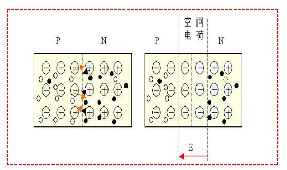
var videoObject = {container:'.video', variable:'player', autoplay: true, html5m3u8: true, video: "https://vdse.bdstatic.com//2b31b07dfbce77278c1747ab39a819fb?authorization=bce-auth-v1%2F40f207be6485424f47b2e3dfbb %2F2017-05-11T09%3A02%3A31Z%2F-1%2F%2F530875472397485e4bb83957c7fe201e01c292dca2aa702b69edbeea8bce047f" }; if (!! window.ActiveXObject) {videoObject.html5m3u8 = false} varvideoObject = new ckplayer( Semiconductor