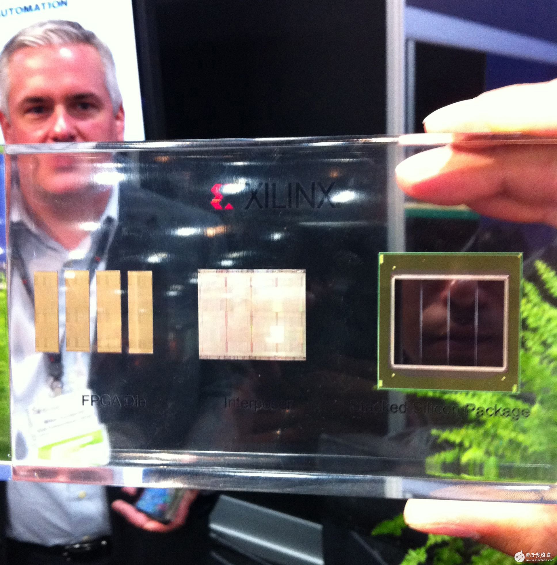
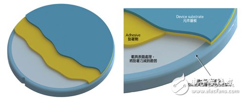
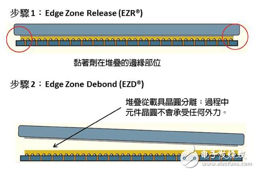
The 2.5D Silicon Interposer (Interposer) is a new interconnect technology that offers many technical advantages for different applications. At this stage, field-programmable gate arrays (FPGAs) have been the driving force behind the development of advanced complementary metal oxide semiconductor (CMOS) silicon interposers, but in fact, silicon interposers have long been used in light-emitting diodes (LEDs) and micro Many applications such as electromechanical systems (MEMS). Multi-step wafer process assists silicon interposer cost reduction One of the most attractive aspects of the 2.5D silicon interposer is the Die ParTITIoning technology. Unlike system-on-a-chip (SoC), which integrates different system functions such as logic, memory or radio frequency (RF) into a single component, the silicon interposer uses a modular approach to place different functions in different crystals. On the grain. Due to the relationship between the microbump and the redistribuTIon layer of the copper process, the electrical characteristics of the chip and the chip through the silicon interposer are very similar to those of the intra-chip interconnect. This can significantly reduce power consumption and increase bandwidth. However, in addition to all technical advantages, the most important factor is still the cost factor. To extend the usability of silicon interposer technology, the key premise is to significantly reduce costs. Here are a few ways to reduce the cost of silicon interposers. The first method is to replace the single crystal silicon wafer (Crystal Silicon Wafer) with polycrystalline silicon or glass to reduce the cost of the substrate; another method is to reduce the cost by increasing the size of the substrate. Both 18-inch wafers and rectangular panels are possible ways to reduce costs. However, both methods can make huge changes and require a completely different process industry system. However, one of the most promising methods available in existing wafer processing systems is to create more process steps in the wafer level process. At present, the general process architecture is to first produce silicon interposer wafers, and then stack the dies on the intermediate silicon interposer; the chip stacking technology on the interposer is the last process step of chip-level integration. Although the process of this known good chip (Known Good Die) is extremely optimistic, it will also cause many process problems. First of all, such a large and very thin silicon interposer grain, its bow and warp (Warp) is a big problem, not only in the processing of the die, but also the alignment and heat. Thermo-compression bonding is also quite difficult. In addition, the subsequent die bonding process is also very slow and therefore also costly. A sensible approach is to use die-wafer-level (C2W) integration for die stacking, which speeds up the process cycle; on the other hand, after chip stacking (such as creating a temperature equalization plate or heat sink) Perform wafer level processing. The thickness of the silicon interposer wafer is very thin based on size and cost considerations. At present, the general thickness is 100 micrometers (μm), which has been able to meet the size considerations. However, the TSV process is a major practice to reduce costs; the cost of making a 10 micron & TImes; 50 micron TSV is much lower than making a 10 micron x 100 micron TSV. Wafer thinning can be accomplished by temporarily bonding the silicon interposer wafer to the carrier wafer and then thinning the wafer back side. The carrier wafer has mechanical support to avoid wafer breakage and compensate for the stress required in the silicon interposer wafer. Reducing the thickness of the wafer is a way to reduce the cost of the silicon interposer, but after the debonding process, the thinner grains are mechanically stable, stressed, and the bow of the silicon interposer. New challenges may arise in the handling of deflections. Among them, the solution to these problems is to perform die-wafer level bonding on a thin silicon interposer wafer while still on the carrier wafer. Subsequent, other steps can be performed at the wafer level. Mass production thinning wafer yield management is very important Yield management is a key factor in dealing with thin wafers. Inconsistent thickness of thinned wafers is a very serious problem. If the thinned wafer is cracked after the thinning process, or the center-to-edge of the wafer is uneven, it will cause expensive cost in the process of exposing the via hole to compensate for the crack on the wafer; or Even more serious is to scrap the wafer because the grinding on the back side of the wafer cannot be repeated. By performing 100% adhesive film quality and overall thickness variation (TTV) inspection on the wafer, you can find various problems before spending a lot of money. Wafer-to-vehicle alignment problems are often overlooked, but this is a very important part of yield management. Recent high-volume production results show that wafer-to-vehicle alignment accuracy has a positive relationship to wafer edge grain yield. The optical edge alignment system allows the wafer to be precisely aligned to the carrier. For the silicon interposer process, the side of the flip-chip bump is usually the first to be produced (at the front end of the interposer), and the microbump is produced on the back side of the thin interposer. The ideal line/space resolution of the redistribution layer is 1 micron / 1 micron, in other words, the repeat alignment aligner (Stepper / Scanner) must be used for lithographic exposure purposes. The inspection range of these systems is very small, and accurate alignment of the wafer and the carrier ensures that the alignment keys are within the exposure window. The exposure machine does not require time-consuming search for the registration key, thus achieving the highest yield. Another important focus of the thin wafer process is the selection of suitable temporary adhesives. The logic, memory, power components, and interposer processes have different requirements for the adhesive. In general, an adhesive will not meet the needs of all applications. New types of adhesives are typically dedicated to memory, logic or power component applications. However, fabs and outsourced package test service providers must also have the ability to support these different application needs, ie they can use different adhesives at the same time. ONE Group's recently launched ZoneBOND technology, a mechanical peeling method at room temperature, provides a breakthrough for suppliers towards an open and diverse development. With this technology, the carrier can have a peeling function. Figure 1 shows the ZoneBOND carrier wafer with a weaker adhesion at the center and the strongest adhesion at the edge. Figure 2 shows the stripping process. First, the adhesive at the edge is dissolved in the single-wafer mode of the Edge Zone Release (EZR) process, and the component wafer is then separated from the carrier wafer in the Edge Zone Debond (EZD) process. Thin wafers for subsequent wafer dicing and packaging processes. The actual stripping process takes place between the carrier wafer and the adhesive film. In this stripping process, the bumps can be safely embedded in the adhesive film, and the bumps are not subjected to any external force during the peeling process. Different adhesive suppliers currently offering ZoneBOND materials have an open common platform to form a diverse supply chain. Figure 1 Amplification of the ZoneBOND vehicle architecture Figure 2 The ZoneBOND stripping process is a two-step process in which the edge portion of the adhesive dissolves during the separation step; the thinned wafer is separated from the carrier during the stripping step. Standardized Processes and Equipment Help Reduce 2.5C IC Thinning Wafer Costs In other words, ZoneBOND technology standardizes the process and allows the adhesive to be independent of the process equipment. Through this technology, the temporary joining and stripping tool can be any adhesive, such as a Spin Coater. Temporary bonding and bonding separation equipment can use any kind of photoresist in the coating process. (Photoresist). Therefore, a variety of different adhesives from a wide variety of manufacturers can be used in the process. Standardization of processes and equipment is key to making the industry system more competitive, which not only helps reduce the cost of thinning wafer processes for 2.5D IC applications, but also brings the same benefits to 3D IC applications.
This Wifi Backup Camera connects wirelessly to your smartphone allowing you to see the camera view on your smartphone screen! Download the free My Cam app from the App Store for IOS device or Google Play Store for Android device , the camera and smartphone will be able to connect via a WiFi connection .
1, Wifi Wireless Backup Camera
system for Truck/Van/Caravan/Trailers/Camper/Pickup/5th Wheel/Bus. Easy
to install, no more complex wiring.
2,Rearview IR Reverse HD backup Camera with Built-in
Wireless Transmitter---with 12/18/28 individual Infrared (IR) LED for Night Vision.
Hard Metal Cased Camera with IP68 Waterproof and Mud proof, Designed and tested
for extreme climates.
3, Voltage Range From 12-32V DC Power, Flexible Vehicle
Compatibility.
4, Digital wireless
technology for specialty vehicles , No any interference with other wireless devices,
if you ensure stable and high resolution image with 100M acceptance range in
open areas.
Wifi Backup Camera Wifi Backup Camera,Wifi Wireless Backup Camera,Wifi Wireless Backup Camera For Suv,Wifi Plate Frame Backup Camera Shenzhen Sunveytech Co.,LTD , https://www.sunveytech.com