1 Introduction Due to the cost of wireless mobile networks, mobile data processing transmission systems should have strong real-time data processing and data compression functions to reduce the amount of data transmitted and received over the mobile network. In addition, because the instrument has the characteristics of small size, portability, long working time, battery power supply, etc., the mobile data processing transmission system is required to have lower power consumption. In order to achieve the above objectives, this paper designs a mobile data processing transmission system based on TI's low-power DSP chip and Cygnal low-power mixed-signal system-level single-chip microcomputer. Figure 1 Mobile Data Processing Transmission System The mobile data processing transmission system (see Figure 1) consists of three main DSP units, a CPU unit, and a GSM unit. After amplification and filtering, the analog signal is sent to the CPU unit for A/D conversion. The CPU unit sends the A/D converted analog signal to the DSP unit through the HPI bus for a variety of high-speed operations such as FFT, wavelet transform, filtering, pattern recognition, and encoding compression. . The result of the operation is sent to the CPU unit via the HPI bus. The CPU unit can also perform simple processing and analysis on the signals sent by the DSP unit. The CPU unit also controls the operation of other auxiliary units (eg, keyboard unit, clock unit, LCD unit, LED unit, etc.). The CPU unit controls the GSM unit to transmit and receive data through the wireless mobile network through the serial port. Therefore, the mobile data processing transmission system is actually a CPU-based data acquisition, processing system and transmission system. Siemens' TC35 series GSM engine module [7] is cost-effective, and has a domestic radio access network card. The TC35 is mainly composed of an RF antenna, internal Flash, GSM baseband processor, matching power supply and a 40-pin Zip socket. The GSM baseband processor is the core component, and its function is equivalent to a protocol processor, which is used to process the AT commands sent by the external system through the serial port. The RF antenna part mainly implements signal modulation and demodulation, and realizes signal conversion between the external RF signal and the internal baseband processor. The matching power supply provides the required power for the processor and the RF part, and the socket is an application interface provided to the user. The TC35's user application interface uses a 40-pin Zip socket, which includes pin functions: 3.3 to 5.5V peak 2A DC power supply; analog audio input and output interface; standard RS232 signal interface, a total of 8 pins; SIM The number of card connection pins is six, which is in line with the GSM11.11 standard. It is particularly important to note that the RS232 interface uses a 9-bit encoding format, of which 8 data bits, 1 stop bit, and no parity bit. Therefore, the MCU generally works in mode 1 and supports a rate of 1200-115200 bps (but standard). GSM networks generally only support a rate of 9.6 Kbps).
Our Driverless LED Flood Light Use Seoul IC drive program,
driverless, ultra-high efficiency 125LM / W, PF> 0.9, no EMI electromagnetic
interference, 10KV Surge Protection, more than 50000 hours lifespan, 5 years
warranty, Mainly used for large-scale workplace mines, building contours,
stadiums, overpasses, monuments, parks and flower beds. Available in 40W, 50W,
100W, 150W, 200W, versions.
Driverless LED Flood Light,LED Flood Light Driverless,Module LED Flood Light,Flood Light Shenzhen Ri Yue Guang Hua Technology Co., Ltd. , https://www.ledlightinside.com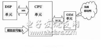
2 DSP unit The DSP unit performs various high-speed operations on the A/D-converted raw data signal sent from the CPU unit via the HPI bus, and the result of the operation is sent to the CPU unit through the HPI bus. The DSP unit can undertake algorithms with high real-time requirements and large computational complexity, such as signal preprocessing, signal detection and classification. Here, the TMS320VC5409[1] chip from TI's TMS320-54 series DSP is used. The TMS320C54X is a fixed-point DSP chip specifically designed for low power, high performance and low cost. The main features of the TMS320C54X include:
(1) The calculation speed is fast. The instruction cycle is 25/20/15/12.5/10ns, and the computing power is 40/50/66/80/100 MIPS;
(2) Optimized CPU structure. There is a 40-bit arithmetic logic unit, two 40-bit accumulators, two 40-bit adders, one 17 & TImes; 17 multipliers and a 40-bit barrel shifter, allowing 16-bit strips. / Unsigned multiplication. There are 4 internal buses and 2 address generators. In addition, a Viterbi accelerator is integrated internally to increase the speed of the Viterbi code.
(3) Low power mode. The TMS320C54X can operate at 3.3V, and the three low-power modes (IDLE1, IDLE2, and IDLE3) save DSP power. The TMS320C54X is ideal for wireless mobile devices.
(4) Intelligent peripherals. In addition to the standard serial port and time division multiplex (TDM) serial port, the TMS320C54X also provides an auto-buffered serial port (BSP) and an HPI (Host Port InteRFace) interface for communication with an external processor.
In addition to the 54X feature, the TMS320VC5409 has a 16-bit 16K on-chip read-only memory, a 16-bit 32K on-chip dual-operation data memory, three multi-channel buffered serial interfaces (McBSPs), and an enhancement. 8-bit host interface (HPI) with 16-bit data/address drive capability [2], a 16-bit timer and 6-channel (DMA) controller operating at up to 100 MIPS, supporting 8 megabytes of external program space, low Power consumption: 3V and 1.8V (core), especially suitable for battery-powered devices.
In a mobile data processing transmission system, the CPU operates in a host mode while the VC5409 operates in a slave mode. The CPU unit controls the RESDSP signal to reset the VC5409 at startup, and the VC5409 user program placed in the DCM8512SRAM (Fig. 5) is transferred to the on-chip high-speed RAM of the VC5409 via the HPI bus during reset to improve the execution speed and power consumption of the DSP. . Since the HINT and INT2 of the VC5409 are connected, when the RESDSP signal is high, the VC5409 bootloader (Bootloader) will be started in HPI[3] mode. The VC5409 will automatically execute the program loaded into the on-chip data memory of the VC5409 by the bootloader. At other times, VC5409 exchanges data with the CPU unit via the HPI bus. In order to meet the needs of real-time digital signal processing, the DSP operates at 100 MHz.
In the case of system power consumption is the primary consideration of system design, DSP devices with low voltage supply should be selected as much as possible. In addition to reducing the power consumption of the DSP itself to reduce the total power consumption of the system, the DSP that selects the 3.3V low-voltage power supply can also reduce the power consumption of the external logic circuit, which plays an important role in achieving low power consumption of the system. Also use the IDLE instruction on the software to reduce power consumption. VC5409 has several power reduction modes of IDLE1, IDLE2 and IDLE3. The IDLE instruction suspends CPU internal operations (suspend acTIvity), but still retains the logic of the internal components, allowing on-chip peripherals such as serial ports to continue to operate. At 50 MHz system clock, the typical current required to execute the IDLE2 instruction is 2 mA. If the IDLE3 instruction is executed when the input clock of the internal part is turned off, the current value is only 20μA. 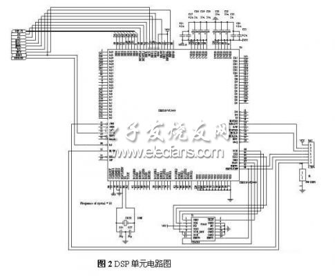
3 Wireless mobile network interface Mobile communication systems mainly use CDMA and GSM standards. The GSM system is the second generation mobile communication system [4]. It provides a variety of services, mainly voice, short message, data services. The GSM system is composed of several sub-systems and can be interconnected with various public communication networks (PSTN public telephone network, ISDN integrated service data network, PSPDN public switched packet data network, etc.), and the GSM system can provide access to international borders. Automatic roaming feature. GSM has two parallel systems: GSM900 and DCS1800. These two systems have the same function, mainly with different frequencies. The GSM mobile communication network can provide a variety of telecommunication services, mainly including:
The telephone service is the most important service provided by the GSM mobile communication network. Real-time two-way voice communication between digital mobile customers, digital cellular mobile telephone network customers, modular cellular mobile telephone network customers, and fixed network customers.
The short message service can be further divided into a point-to-point short message service including a mobile station start and a mobile station termination, and a point-to-multipoint cell broadcast short message service. Point-to-point short message service allows GSM clients to receive short messages sent by other GSM clients. The peer-to-peer short message service is stored and forwarded by the short message service center. Point-to-point information transmission or reception can be performed while the MS is in a call state (voice or data), or in an idle state. When it is transmitted within the control channel, there is no connection established, so the service charge is low, but the amount of information is limited to 140 octets (7-bit code, 160 characters).
In order to meet the needs of GSM mobile customers for data communication services. The GSM system not only enables data communication between mobile customers, but also enables the GSM mobile communication network to communicate with other public data networks. GSM provides asynchronous data transmission capabilities of 2400 bps, 4800 bps, and 9600 bps.
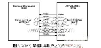
The command interface provided by the GSM engine module complies with the GSM07.05 [5] and GSM07.07 [6] specifications. The AT Command interface defined in GSM07.07 provides a common interface between a mobile station (MS) and a data terminal equipment (DTE). The instruction set is jointly developed by Nokia, Ericsson, Motorola and HP for the GSM system. GSM07.05 provides detailed rules for short messages. When the short message module receives the short message sent by the network, the short message can send the indication message through the serial port, and the data terminal device can send various commands to the short message module. At present, the modules that have been used in China are Falcom series, Wavecom series, Siemens series modules, and the functions and usages of these modules are not much different. The method of transmitting data in the GSM network by using the GSM engine module, combined with the existing system through the RS232 interface (Fig. 3), can use only two lines of TXD and RXD to realize wireless transmission of data. And the existing system hardware part does not need to make major changes, the key is to modify the software part.