Design of Power Line Communication Analog Terminal Based on TMS320LF2812
This article describes a system that implements a power line modem from software and hardware in compliance with the CEA709 protocol using a fixed-point DSP controller (TMS320LF2812). The specific design method of the analog terminal is described in this paper, and this terminal is necessary for the stable transmission and reception operation process.
1 System framework based on CEA709 protocol
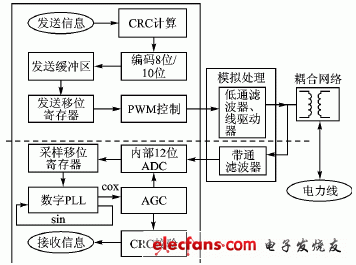
Figure 1 shows the physical block diagram of the ANSI/CEA709 protocol standard.
LonWorks, a widely used control network platform in the fields of rail transit, network energy management, intelligent buildings, HVAC, coal mine safety, energy and environmental management, has become the guiding technical document of China's national standards. The global building, home, industrial and transportation automation industries are currently heavily based on the LonWorks platform. The LonWorks platform is the core technology platform for the world's largest residential smart meter network. It is used by smart meters for residential and small commercial electricity meters in countries such as Sweden, the Netherlands and Australia. The protocol running on this platform is the US control network standard ANSI/ CEA709. At present, more and more Chinese manufacturers and integrators have adopted the ANSI/CEA709 protocol standard, for example, on the Qinghai-Tibet Railway, the world's longest high-altitude railway train, using the LonWorks technology platform, using the ANSI/CEA709 protocol. Used for technical monitoring and control of various systems, including monitoring of the most advanced passenger oxygen supply systems.
For the CEA709 physical layer block diagram in Figure 1, the system block diagram of the DSP to implement the CEA709 modem function is shown in Figure 2. The DSP (TMS320F2812) has 150 MIPS of computing power. The signal acquisition uses a 12-bit on-chip analog-to-digital converter with a conversion speed of 12 Msps. The DSP provides multiple PWMs to accommodate the power line modem.
Figure 2 system block diagram
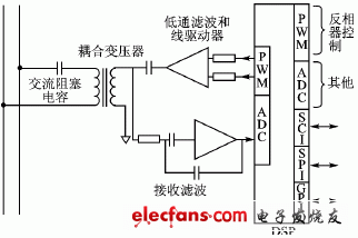
Two on-chip PWM outputs and one line driver are used to implement the modem's transmit function. An A/D input is used to sample the bandpass input port signal to implement the receiver's receive function. The bandpass filter is actually a discrete filter. They complete the analog front end design of the interface with the AC blocking capacitor and the coupling transformer.
The following mainly introduces the design process of the analog front-end interface.
PCB SMT Stencil ,the unique goal is to move solder paste to the bare Printed Circuit Board.
PCB Stencil , SMT Stencil, SMD Stencil , Laser Stencil , What is it?
Apart from all types of Printed Circuit Boards (PCBs) such as Prototype PCB , Aluminum PCB , HDI PCB , Flexible PCB , Rigid Flex PCB , Thick Copper PCB, High TG PCB , JHYPCB also manufactures solder paste stencils to meet Surface Mount Technology (SMT) requirements.
PCB Stencils, also called SMT stencils, SMD stencil, play a key role in transferring accurate amount of solder paste to correct positions on bare circuit boards ready for assembly. In other words, stencils can fast and efficiently ensure the most accurate solder paste amount and optimal electrical connection. With solder stencils, it is possible to use metal squeegee blades to apply solder paste easily over the openings on PCBs and make stencil to be well aligned with the surface of the advanced circuit board.
All of our SMT Stencils stencils are 100% laser-cut type 304 full-hard stainless steel, ensuring the finest quality finish on the market today. We use a .001" laser beam with 98% overlap creating an extremely smooth hole that provides the best paste release. Most stencil fabricators use a .003" laser leaving mouse bites on the aperture edge. You can choose a PCB Prototype stencil, a frameless foil stencil, or a rigid permanently mounted stencil. Both the frameless and framed stencils come in various sizes to accommodate your printer and stencil requirements.
PCB Stencil Types Available:
1. Laser-cut stencils
The openings are lasered on 100% stainless steel. Generally speaking, this kind of stencil can be produced with high quality and a high degree of precision within a short time.
Advantages: high accuracy; barely influenced by objective elements; trapezoid opening beneficial for demoulding; suitable for accurate cutting; reasonable price;
Disadvantages: relative low manufacturing speed.
2. Chemical-etch stencil
The openings are etched into the metal using acid. Usually this kind of stencil offers better protection on material temper and hardness.
Advantages: one-time formation; relatively high manufacturing speed; low cost;
Disadvantages: tending to form sand clock shape or large openings; numerous manufacturing stages and accumulating errors; unsuitable for fine pitch stencils; bad for environmental protection.
3. Prototype PCB Stencil (Low-volume manual printing. Ideal for prototypes)
When prototyping dictates fast action with minimal cost, our prototype stencils are the best solution. Prototype Stencils gives you a quality stencil and framework so you can handle assembly from the convenience of your own desk.
Prototype SMT Stencil Features:
Eliminate the registration difficulty associated in hand printing with a flat piece of metal
Eliminate printer set up for short run prototypes
Allow quick alignment for repeatability
Save money over full size stencils designed for automated printers<
Squeegee included
Prototype
SMT Stencil Specs:
Technology
100% laser cut
Material Used
Stainless Steel
Stencil
Thickness
0.06 ~ 0.3 mm
Minimum Cut
Width
0.05 mm
Maximum Size
736 X736 mm
Aperture
Tolerance
within 0.007mm
Allow for
Fiducial Data
Yes
Delivery
1 ~2 Day
4. NEW Prototype PCB Stencil Kit (with leaded or lead/free solderpaste)
Includes Prototype Stencil, one board holder, leaded or lead-free solder paste (must specify), temperature marker, squeegee, ESK-safe gloves and alcohol wipe.
5. NEW Pick and Place Tool
Handy and convenient for low quantity prototype assembly using the Prototype Stencils. Re-usable, includes vacuum bulb and vacuum clips with diameters of 3/8", 1/4", and 1/8".
6. Framed SMT Stencils (Also called "Glue-in" or Mounted Stencils)
Framed stencils are laser-cut stencils designed for high volume screen-printing. With a framed stencil, your stencil is securely mounted to either a cast or extruded aluminum stencil frame a stencil frame using a mesh border, allowing for complete control.
Framed SMT Stencil Features:
Unique Process for smooth aperture walls
Very clean laser-cut apertures
Excellent print performance
Excellent for high-volume stencil printing on printed circuit boards
Unique process creates permanent non-removable non-fading fiducial
All framed SMT stencils are double bonded to extreme wear
24-hour turnaround standard
Framed
SMT Stencil Specs:
Technology
100% laser cut
Material Used
Stainless Steel
Frame Types
Cast, Space Saver
Stencil
Thickness
0.06 ~ 0.3 mm
Minimum Cut
Width
0.05 mm
Maximum Size
736 X736 mm
Aperture
Tolerance
within 0.007mm
Allow for
Fiducial Data
Yes
Allow for
Panelized Data
Yes
Delivery
1 ~2 Day
Framed PCB Stencil Specification
Framed PCB Stencil Area
Maximum Squeegee Area
300mm*400mm (11.81inch*15.75inch)
120mm*220mm (4.72inch*8.66inch)
370mm*470mm (14.57inch*18.5inch)
200mm*300mm (7.87inch*11.81inch)
400mm*600mm (15.75inch*23.62inch)
220mm*400mm (8.66inch*15.75inch)
400mm*700mm (15.75inch*27.56inch)
220mm*500mm (8.66inch*19.69inch)
400mm*800mm (15.75inch*31.5inch)
220mm*600mm (8.66inch*23.62inch)
400mm*900mm (15.75inch*35.43inch)
220mm*700mm (8.66inch*27.56inch)
400mm*1000mm (15.75inch*39.37inch)
220mm*800mm (8.66inch*31.5inch)
400mm*1200mm (15.75inch*47.24inch)
220mm*1000mm (8.66inch*39.37inch)
400mm*1400mm (15.75inch*55.12inch)
220mm*1200mm (8.66inch*47.24inch)
420mm*520mm (16.54inch*20.47inch)
240mm*340mm (9.45inch*13.39inch)
450mm*550mm (17.72inch*21.65inch)
270mm*370mm (10.63inch*14.57inch)
500mm*800mm (19.69inch*31.5inch)
320mm*600mm (12.6inch*23.62inch)
500mm*1200mm (19.69inch*47.24inch)
320mm*1000mm (12.6inch*39.37inch)
550mm*650mm (21.65inch*25.59inch)
340mm*440mm (13.39inch*17.32inch)
584mm*584mm (23inch*23inch)
380mm*380mm (15inch*15inch)
736mm*736mm (29inch*29inch)
480mm*480mm (19inch*19inch)
7. Frameless SMT Stencil - Foil/Plate Only (for universal frames)
Foil or Plate Only stencils are designed to work within interchangeable plate or "universal" systems. Also referred to as "reusable", these stencils do not need to be permanently glued into a frame.
Frameless SMT Stencils also referred to as foils are laser cut solder paste stencils designed to work with stencil tensioning systems known as reusable stencil frames. This type of stencil does not need to be permanently glued in a frame. Frameless stencils are significantly less expensive than framed stencils and provide money-saving storage while still delivering superior quality and performance.
Smooth aperture walls, can be used for 16 Mil pitch and below and for Micro BGA's
24-hour turnaround standard
Frameless
SMT Stencil Specs:
Technology
100% laser cut
Material Used
Stainless Steel
Stencil
Thickness
0.06 ~ 0.3 mm
Minimum Cut
Width
0.05 mm
Maximum Size
280 X 380 mm
Allow for
Fiducial Data
Yes
Allow for
Panelized Data
Yes
Delivery
1 ~2 Day
8. Frameless SMT Stencil - Foil/Plate Only (for hand printing)
For times when you need precise control for smaller production runs, our Foil or Plate Only stencils are ideal. These frameless stencils allow you to hand print with precision just the amount you need and can be stored conveniently.
9. Electroformed SMT Stencils
Electroformed SMT stencils are nickel-based, electroform foils permanently mounted in a stencil frame using a mesh border to tightly stretch the stencil foil taut in the frame. Electroformed stencils offer the best paste release characteristics available and are frequently used for fine pitch (20 mil to 12 mil pitch) SMT applications on printed circuit boards. They are also used for µBGA's, Flip Chip, and Wafer Bumping (12 mil to 6 mil pitch).
Electroformed SMT Stencil Features:
The smooth trapezoidal sidewalls of an electroformed stencil allow for better paste release
Nickel has a lower coefficient of friction compared to stainless steel
Electroform foils are harder than full hard stainless steel of comparable thickness, providing for longer stencil life
What's the difference between a framed stencil and a frameless stencil?
A framed PCB stencil will have a 0.5" to 1.5" thick metal frame around it, similar to a picture frame. Framed stencils are often used by contract manufacturers, assembly and board houses, and large scale production facilities and are commonly placed in a manual or automated stencil printing machine. Frameless stencils are a thin sheet of material cut with a small border around your design. For example pictures on these products, please visit our Gallery.
What's the difference between Polyimide and Stainless Steel?
All stencils are made with high quality Polyimide and Stainless Steel. We use only the industry leading Stainless Steel, designed specifically for stencils. These materials are ideal for prototype or Multilayer PCB .
Polyimide has a lower precision rate due to the way it is processed and its ability to withstand heat during the cutting process. Minor variances will occur when the material reacts to the laser. Paste release is great, but this material should be limited to a small number of uses and with components 0402 or bigger.
The minimum aperature size for Polyimide is 0.005" vs 0.001" for Stainless Steel. Polyimide also has a natural curl in the material caused by the way the film is manufacturered, this is outside of our control. Stainless Steel provides the ultimate in precision and quality, with a 0.0007" spot size, and exceptional paste release with a truly flat surface. If you want the absolute best reflow experience, there is no comparison, Stainless Steel is the superior material.
Analysis and Treatment of Common Problems in PCB SMT stencil
Insufficient solder paste
Insufficient solder paste may cause poor bonds and contact between components and the board. The common causes of insufficient solder paste are poor gasketing, clogged stencil apertures, insufficient solder paste bead size, paste/stencil being used beyond recommended life span, stencil not wiped clean, or low squeegee pressure.
Smudging/bridging
The main causes of smudging/bridging are excessive squeegee pressure, inadequate stencil wiping, poor contact between the board and stencil, high temperature or humidity, or low solder paste viscosity.
Misalignment print
A typical misalignment print is usually caused by the vision system not spotting fiducials, PWB or stencil stretch, poor contact between the board and the stencil, or weak board support.
Bow and twist
A PCB Board not fixed properly during solder paste printing gives poor results and increases soldering related issues. Normally, solder paste printing equipment can handle warpage of 1.0 to 3.0 mm but beyond this limit needs some special jigs or fixtures to hold the PCB. It may be difficult to tackle thick and small boards compared to thin and bigger size boards.
How to Determine Stencil Size?
Stencil size is composed by two parts: internal size and overall size. Internal size is the size compatible with that of PCB ready to be assembled while overall size refers to the size compatible with printer parameter limit. As long as both sizes are accurately designed, stencil will be able to make full use of its functions.
Internal size of stencil can be figured out conforming to the following rule:
Width of Framed Stencil = width of PCB + 100mm while its Length = length of PCB + 100mm
Width of Frameless stencil = width of PCB + 200mm while its Length = length of PCB + 200mm
For example, if one circuit board size is 50*50mm, then the size of its framed stencil should be around 150*150mm and the size of its frameless stencil should be around 250*250 mm.
It's easy to remember and operate so it worked for manual solder paste printing in SMT assembly prior to the advent of automatic printer. It can be said that different PCB sizes lead to generations of different internal sizes of stencil.
When it comes to automatic solder paste printer, however, it's relatively solid. Overall size of stencil has to be determined by parameter limit of the equipment, that is, printer, because stencil has to work within the range of printer with a frame. Different printers feature different parameter regulations. As far as PCBCart is concerned, the stencil size compatible with our printer can be either 650mm*650mm or 736mm*736mm.
PCB designers have to focus on internal size of stencil, they don't need to care about its overall size since it is generally determined by the parameters of printer in your contract assembler workshop.


")


