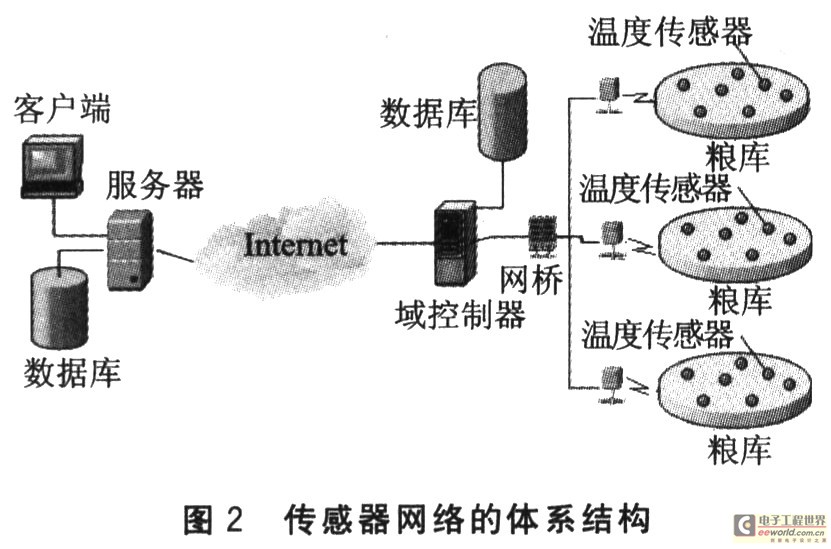
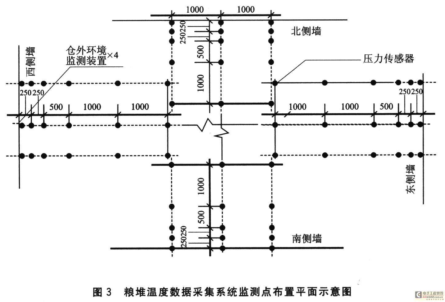
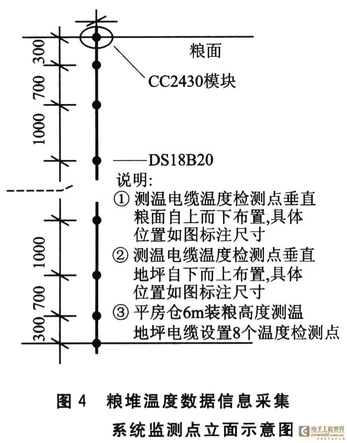
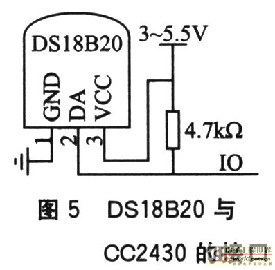
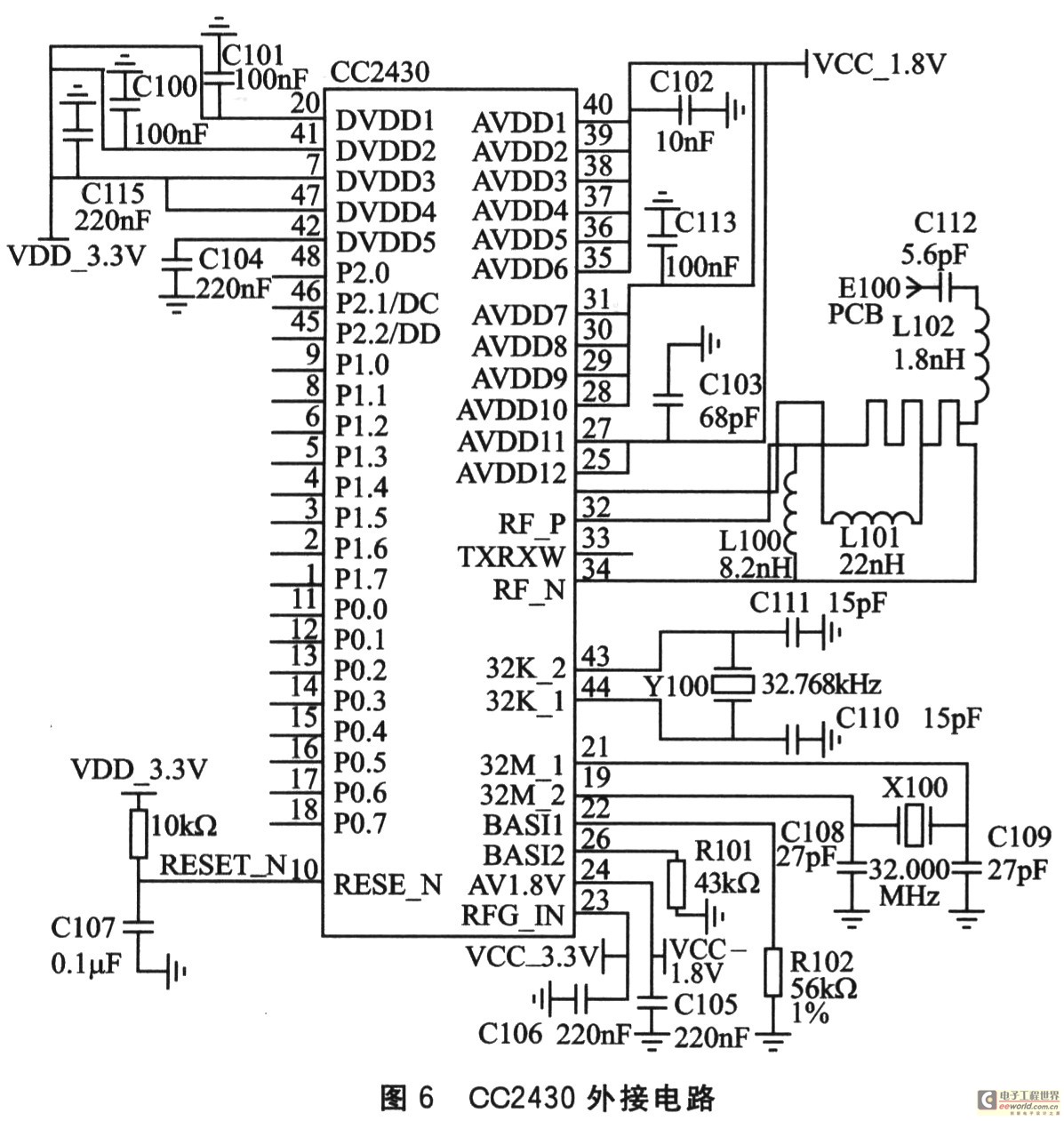
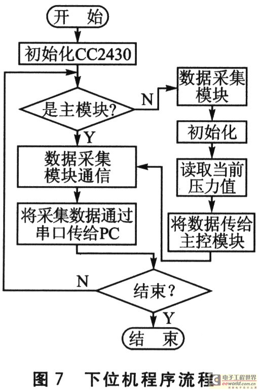
CC2430 and DS18B20 Grain Depot Temperature Sensor Network Design 1 Sensor network architecture A typical sensor network architecture includes distributed sensor nodes, gateway nodes, the Internet, and user interfaces. In the sensor network, the nodes are arranged in the monitored area. Each sensor network is equipped with a gateway connected to the transmission network. The gateway transmits the measured data from the sensing area to the base station providing remote connection and data processing through the transmission network, and the base station is connected to the remote database through the Internet. The final collected data is provided to the end user through an interface after analysis and mining. The main structure of this system is that each CC2430 module is connected with multiple DS18820 temperature sensors. The temperature sensors are arranged in the grain depot according to a certain rule, and connected to the current CC2430 module through a single bus; these CC2430 modules are networked using wireless sensor network networking technology, and the data is sent to the local data concentrator, and the data is transmitted through the network bridge The concentrator is connected to the local monitoring host, as shown in Figure 1. Finally, the remote terminal users are connected to the local monitoring system through the Internet to realize the remote networked grain depot quantity monitoring, as shown in Figure 2. 2 Sensor placement model The schematic diagram of the layout of the monitoring points of the temperature data information collection system of the flat warehouse grain pile is shown in Figure 3. The temperature sensor in the warehouse is set with three groups of temperature sensors on each side of the east, south, west and north walls, each of which is 1 m apart; the east, south, west and north sides are inward from the wall The spacing of the arrangement is 0.25 m, 0.25 m, 0.5 m, 1.0 m, 1.0 m ... The schematic diagram of the elevation of the monitoring point of the temperature data information collection system of the bunker warehouse grain pile is shown in Figure 4. The temperature monitoring points of the grain pile are arranged from the grain face down and from the silo bottom up respectively. Eight temperature sensors are set for each single bus cable according to the grain height of 6m. The distance between the grain grain down and the silo bottom up sensors is 0.30 m , 0.70 m, 1.0 m, 1.0 m. The data information of the three grain pile temperature monitoring points on the same plane on the east, south, west and north sides of the warehouse are averaged to improve the reliability and accuracy of the monitoring data information. 3 DS18B20 single bus temperature sensor The DS18820 digital thermometer provides 9-bit (binary) temperature readings, indicating that the temperature information of the device is sent to or sent from the DS18820 through the single-wire interface, so only one wire (and ground wire) is needed from the host CPU to the DS18820. The power of DS18820 can be provided by the data line itself, without the need for external power. Because each DS18820 has been given a unique serial number at the factory, any number of DS18820 can be stored on the same single-wire bus, which allows temperature-sensitive devices to be placed in many different places. The measuring range of DS18820 is from -55 ℃ ~ + 125 ℃, the increment value is 0.5 ℃, and the temperature can be converted into a number within 1 s (typical value). The interface circuit of DS18820 and CC2430 is shown as in Fig. 5. The temperature reading process of multiple DS18820s is as follows: reset → send 55HMATCHROM command → send 64-bit address → send 44H start conversion command → delay → reset → send 55HMATCHROM command → send 64-bit address → send 0BE read memory command → read 2 words continuously Section data (ie temperature) → reset → read the next device temperature. 4 CC2430 module 4. The main characteristic of CC2430 chip The CC2430 chip continues the architecture of the previous CC2420 chip, integrating the ZigBee radio frequency (RF) front end, memory, and microcontroller on a single chip. It uses an 8-bit MCU (8051), with 128 KB of programmable flash memory and 8 KB of RAM, and also contains an analog-to-digital converter (ADC), several timers (TImer), AES128 coprocessor, watchdog timing (WatchdogTImer), sleep mode timer of 32 kHz crystal, power on reset circuit (power on reset), brownout detection circuit (brown out detecTIon), and 21 programmable I / O pins. The CC2430 chip is produced using a 0.18 μm CMOS process; in the receiving and transmitting modes, the current consumption is lower than 27 mA or 25 mA, respectively. The CC2430's sleep mode and ultra-short time transition to active mode are particularly suitable for applications that require very long battery life. The main features of the CC2430 chip are as follows: high-performance and low-power 8051 microcontroller core; integrated 2.4GHz RF radio transceiver that conforms to the IEEE 802.15.4 standard; excellent wireless receiving sensitivity and strong anti-interference ; In sleep mode, only 0.9μA current consumption, external interrupt or RTC can wake up the system; in standby mode less than 0.6μA current consumption, external interrupt can wake up the system; hardware supports CSMA / CA function; Wide voltage range (2.0 to 3.6 V); digital RSSI / LQI support and powerful DMA function; battery monitoring and temperature sensing function; integrated 14-bit analog-to-digital conversion ADC; integrated AES safety protocol Processor; with 2 powerful USARTs that support several sets of protocols, and 1 MAC timer in accordance with IEEE802. 15.4 specifications, 1 conventional 16-bit timer and 2 8-bit timers; powerful and flexible Development tools. 4. 2 CC2430 module design CC2430 chip requires few peripheral components to realize the signal receiving and sending function. The circuit uses an unbalanced antenna. Connecting an unbalanced transformer can make the antenna perform better. The unbalanced transformer in the circuit is composed of capacitor C112 and inductors L102, L100, L101 and a PCB microwave transmission line. The entire structure meets the requirements of RF input / output matching resistance (50 Ω). The internal T / R exchange circuit completes the exchange between LNA and PA. A 32 MHz crystal resonator (X100) and two capacitors (C108 and C109) form a 32 MHz crystal oscillator circuit. A 32.768 kHz quartz resonator (Y100) and two capacitors (C110 and C111) are used to form a 32.768 kHz crystal oscillator circuit. The voltage regulator supplies power to all pins and internal power supplies that require 1.8 V. C115, C100, C101, C104, C102, C113, C103, C107, C106, and C105 capacitors are decoupling capacitors used for power supply To improve the stability of the chip, R101 and R102 provide accurate bias resistance for the current, as shown in Figure 6. 5 Software design 5.1 Computer software design In this system, the upper-layer management software adopts a 3-layer C / S mode to process the data sent by the sensor network in real time to form the data representation form that the user ultimately cares about. After being authorized, the end users in the local area network can read the real-time data on the monitoring host to realize remote monitoring. The monitoring application software also tracks and manages each node in the sensor network. For the abnormal conditions monitored, the upper management software uses real-time alarm methods of sound and light, SMS, and telephone. It can display parameter lists, real-time graphs (corresponding to specific values ​​and adjust coordinates arbitrarily), real-time data, conversion data, cumulative data, history, alarm screens, reports and other displays. The statistical function can be specifically designed according to user needs. 5.2 Software design of lower computer In the network, each node has a fixed address. The sensor node connected to the monitoring host is a special node, which uses a serial interface to communicate with the monitoring host. The data transmission adopts the master-slave station mode, the node connected with the monitoring host serves as the master station, and controls the communication timing within the network; other nodes as slave stations can be addressed by the master station. The master node mainly completes the collection of data from each slave node and performs preprocessing; the slave node mainly completes the collection of various sensor raw data, as shown in Figure 7. 6 Conclusion The wireless temperature sensor network uses the low-cost, low-power wireless single-chip CC2430 as the core, and uses the DS18820 temperature sensor to obtain data. The circuit has a simple circuit structure, stable and reliable operation, high detection accuracy, and is flexible and convenient for wireless data communication. It is particularly suitable for Industrial site environment, monitoring enclosed spaces and other special occasions that require multi-point monitoring. The application of this network has greatly improved the management level of central grain reserves, reduced management costs, and improved the safety of grain depots. To satisfy the increasing demand of gigabit Ethernet POE Switch(GbE) networking, we have developed this series of gigabit Ethernet POE switch. Fast Ethernet POE Switch,8 Port Switch,Fast Ethernet Switch POE,Managed Switch,Gigabit POE Switch, POE Switch Gigabit Shenzhen N-net High-Tech Co.,Ltd , http://www.nnetswitch.com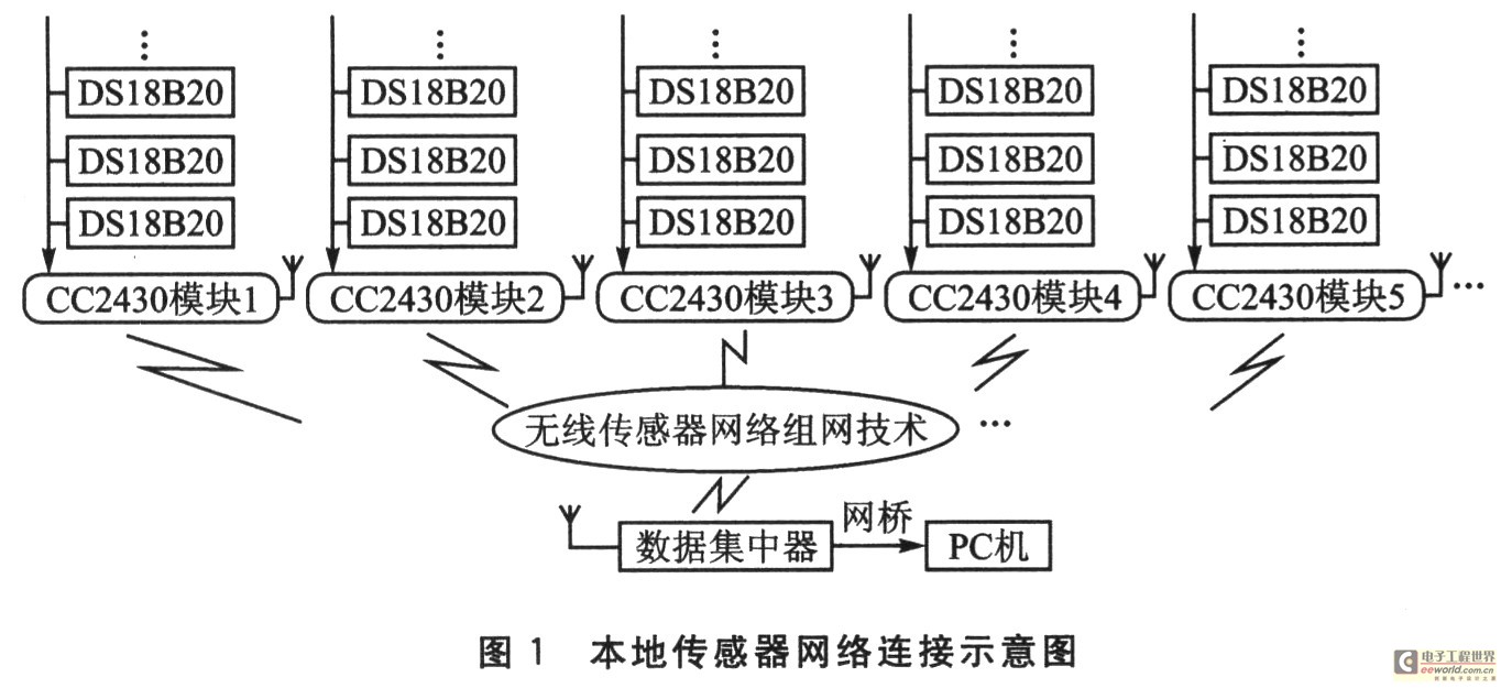
The gigabit Ethernet POE switch supports 120-watt PoE budget to drive up to 4 IEEE 802.3at compliant powered devices simultaneously. The PoE feature enables the NT-WG500-AT4 an efficient and cost-effective solution for SMB, SOHO and other similar fields to deploy the PoE network for wireless access points, IP-based surveillance cameras or IP phones anywhere easily and efficiently.